
FPGA (Field Programmable Gate Array) has seen a rapid growth in the recent years. This post will discuss about what is FPGA (Field Programmable Gate Array), its architecture, how it works,its applications, advantages and disadvantages.
What is Field Programmable Gate Array (FPGA)
Field Programmable Gate Array is system level Integrated Circuit (IC) that helps to create customized digital logic. They are electrically programmed silicon devices which are pre-fabricated. It incorporates millions of logic gates in a single chip. FPGA is a programmable hardware which consists of arrays of Logic Blocks. It can be reconfigured many times as it uses dedicated hardware.
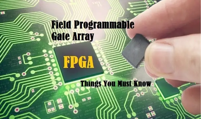
Fig. 1 – Introduction to FPGA
Field Programmable Gate Array has become a preferred implementation media for digital circuits. The programmable Logic and Interconnection Matrix makes them flexible. FPGA’s provide cost-effective solution and quick to market as compared to ASIC’s.
Configuration of Field Programmable Gate Array (FPGA) takes less than a minute and offers Parallel processing i.e. portion of FPGA can be reconfigured while the rest of FPGA is running to implement other functionality. Both the functionality that is configured will execute at the same time.
It is based on Look Up Tables which can implement any Boolean functions.  It consists of programmable SRAM, high-speed input/output pins (I/O), Logic Blocks and Interconnection Matrix. Xilinx in the year 1985 combined the idea of Programmable Logic Devices and Gate Arrays to discover FPGA’s.
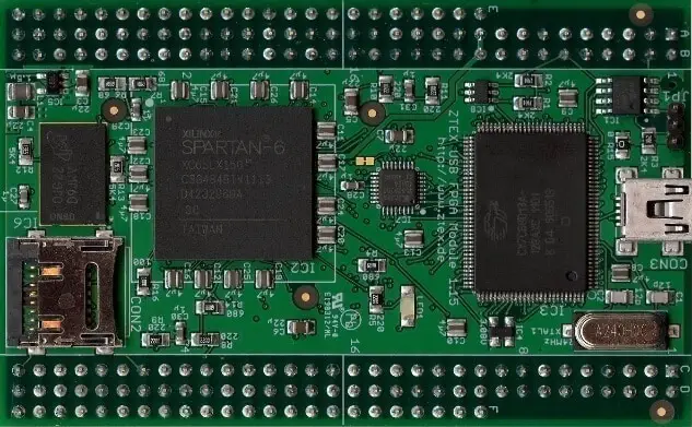
Fig. 2 – Field Programmable Gate Array (FPGA) Development Board
Architecture of Field Programmable Gate Array (FPGA)
The architecture of Field Programmable Gate Array comprises of three main components. They are:
- Programmable Logic Blocks (Configurable Logic Blocks)
- I/O Blocks (Input/output Blocks)
- Interconnection Matrix
Programmable Logic Blocks (Configurable Logic Blocks)
Programmable or Configurable Logic Blocks help in implementing Logic functions. This module provides basic logic and storage functionality. They are arranged in a two-dimensional grid and are interconnected by routing wire segments as shown in the Fig. 3.
The density of the logic block depends upon the length and number of wire segments used for Routing. Configurable Logic Block may consist of single Basic Logic Element (BLE) or clusters of BLE which are interconnected. BLE consists of LUT (Look Up Table), Flip-Flop and Multiplexer as shown in the Fig. 3.
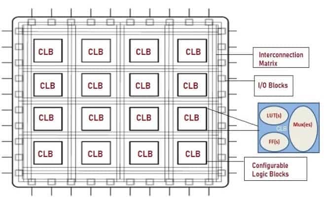
Fig. 3 – Architecture of Field Programmable Gate Array (FPGA)
I/O Blocks (Input/output Blocks)
I/O Blocks consists of interfacing pins which helps in connecting Logic blocks to external components. They are located at the periphery of the grid and also connected to the Interconnection Matrix.
Interconnection Matrix
The function of Routing the signals and providing connections between the Logic Blocks and I/O Blocks is the task of Interconnection Matrix. It consists of wires and switches to establish the connection within FPGA.
How does Field Programmable Gate Array (FPGA) Work
FPGA’s are used as functional blocks in a system which are initially not configured. They are prefabricated and customized according to the application. Configuration is achieved through programming, using VHDL (Very High Definition Language) or Verilog by the end user. The configuration is done through SRAM cells, EPROM or EEPROM.
FPGA reads its configuration from its memory. Logic function is compiled using a software on a computer. Binary file is synthesized and programmed on to FPGA chip for logic emulation.
SRAM based FPGA’s are widely used in varied applications and hence let us focus on the working principle of SRAM-FPGA’s. In this type, memory cells are scattered throughout Field Programmable Gate Array. SRAM (also called Static Random Access Memory) is used to store the programmed value.
Let us consider Fig.4 which shows schematic representation of Configurable Logic Block. Basically, FPGA’s use LUT’s (Look Up Tables) for creating digital logic. This structure contains LUT’s which are used to map input values to output values. Logic Block has programmable Flip-Flop’s and multi programmable Multiplexers.
Look Up Tables are configured using Bit-stream to implement Boolean function. It has four inputs A, B, C, D and the 16 inputs to the Multiplexers determine the Boolean function to be implemented based on the entries of the Truth Table.
These 16 binary values are stored in Registers i.e. D Flip-Flop. These Registers are either set to Logic High or Low. The entire circuit behaves like a 16:1 Mux. If input bits ABCD is 0000, then MSB or top-most input of Mux is routed to output ‘Y’. Truth Table is constructed for different values of input bits. For 4 input bits, there are 16 entries and output ‘Y’ is recorded and verified. LUT-4 uses 16 SRAM bits to implement 4 inputs Boolean Function.
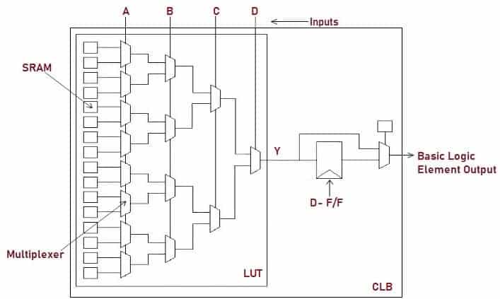
Fig. 4 – Schematic Representation of Configurable Logic Block
Similarly, LUT with k inputs (LUT-k) contains 2k configuration bits and it can implement any k-input Boolean function. Thus, this structure effectively implements arbitrary, complex digital logic.
Let us take an Example of 2 input LUT, that implements the function:
![]()
a and b are the inputs. For different values of the inputs, Truth Table is created. Four entries of the Truth Table are shown in the Fig. 5.
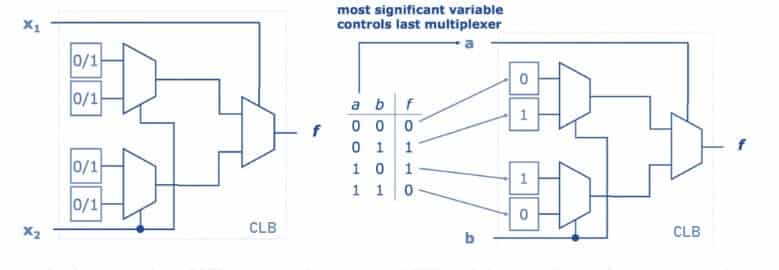
Fig. 5 – Schematic Representation of Two Input LUT
Applications of Field Programmable Gate Array (FPGA)
The applications include:
- FPGA’s are widely used for defense applications like Radar and Sonar.
- Medical imaging implementation requires Field Programmable Field Array.
- They are primarily used in Real-time speech recognition systems.
- They are also used in Avionic systems as they are economical compared to Microprocessors and Microcontrollers.
- They are used in Crypto Systems.
- They are used in ASIC Prototyping.
- They are used in Automotive infotainment applications.
- They are extensively used in Life Science applications like Genome Sequencing.
- FPGA’s are used in Data Analytics applications.
- They are used in Video Transcoding.

Fig. 6 – Applications of FPGA
Advantages of Field Programmable Gate Array (FPGA)
The advantages include:
- Prototype implementation is fast and reliable.
- Operation speed is high.
- Offers reconfiguration and hence they are reusable.
- FPGA’s offer flexibility in design.
- Performance is high i.e. larger data can be processed with fewer clock cycles at high frequencies.
- They are capable of Parallel Processing.
- FPGA’s are economical.
- They operate faster than ASIC’s (Application Specific Integrated Circuits).
Disadvantages of Field Programmable Gate Array (FPGA)
The disadvantages include:
- Programming is complex.
- Power consumption is high.
Also Read:
Smart Street Light System: Architecture, Working Principle, Applications
Solar Power Satellite – How it works, Architecture, Application, Advantage
Random Number Generator – Type, How it Works, Architecture, Application
Can you be more specific about the content of your article? After reading it, I still have some doubts. Hope you can help me.
Thanks for sharing. I read many of your blog posts, cool, your blog is very good.
I was reading through some of your blog posts on this internet site and I believe this site is rattling informative ! Continue putting up.
8ni1tf
Youre so cool! I dont suppose Ive learn anything like this before. So good to search out any individual with some unique thoughts on this subject. realy thanks for beginning this up. this web site is something that’s wanted on the web, someone with a little originality. useful job for bringing one thing new to the internet!
Hello there, You’ve done a fantastic job. I will definitely digg it and in my opinion recommend to my friends. I am sure they’ll be benefited from this website.
Hello.This article was really motivating, particularly because I was searching for thoughts on this subject last week.
I’ve been absent for a while, but now I remember why I used to love this blog. Thanks , I¦ll try and check back more often. How frequently you update your web site?
As a Newbie, I am permanently browsing online for articles that can help me. Thank you
Helpful info. Fortunate me I found your website by chance, and I’m shocked why this accident didn’t came about earlier! I bookmarked it.
Rattling fantastic info can be found on blog.
Absolutely written content material, appreciate it for entropy.
Those are yours alright! . We at least need to get these people stealing images to start blogging! They probably just did a image search and grabbed them. They look good though!
What¦s Going down i’m new to this, I stumbled upon this I’ve discovered It absolutely helpful and it has aided me out loads. I’m hoping to give a contribution & help different customers like its helped me. Good job.
Valuable info. Lucky me I found your site by accident, and I’m shocked why this accident didn’t happened earlier! I bookmarked it.
Thanks for the tip! I now have a better understanding of how FPGAs are used in electronics and embedded systems.
I’ve been browsing on-line greater than 3 hours lately, but I by no means found any interesting article like yours. It’s lovely value sufficient for me. In my opinion, if all webmasters and bloggers made excellent content as you did, the web will be much more useful than ever before.
You are my inspiration , I own few blogs and sometimes run out from to post : (.
Keep functioning ,splendid job!
I really like your writing style, good information, thankyou for posting : D.
I think you have observed some very interesting details , thankyou for the post.
When I initially commented I clicked the “Notify me when new comments are added” checkbox and now each time a comment is added I get several emails with the same comment. Is there any way you can remove people from that service? Many thanks!
Super-Duper site! I am loving it!! Will be back later to read some more. I am taking your feeds also
Heya i’m for the first time here. I found this board and I find It really useful & it helped me out much. I hope to give something back and help others like you aided me.
I was just seeking this info for a while. After 6 hours of continuous Googleing, at last I got it in your site. I wonder what’s the lack of Google strategy that do not rank this kind of informative websites in top of the list. Usually the top websites are full of garbage.
中職戰績粉絲必備的資訊平台,提供最即時的中職戰績新聞、球員數據分析,以及專業的比賽預測。
I’m still learning from you, but I’m improving myself. I absolutely enjoy reading all that is written on your blog.Keep the posts coming. I loved it!
como ganar apuestas en vivo
Thanks for some other informative blog. The place else may just I am getting that type of info written in such an ideal manner? I have a venture that I’m simply now running on, and I’ve been on the glance out for such info.
You really make it appear so easy together with your presentation however I to find this topic to be actually something that I feel I might by no means understand. It sort of feels too complex and very large for me. I’m looking ahead in your subsequent put up, I will try to get the grasp of it!
apuestas combinadas para hoy
apuestas deportivas seguras para hoy
apuestas seguras para hoy fútbol
sportwetten test vergleich
sportwetten südamerika strategie
sportwetten bild tipps
wettquoten biathlon
doppelte chance wetten erklärung
wetten online
Good way of telling, and nice post to take information regarding my presentation subject, which i am going to
present in college.
fully cashable no deposit bonus canada, are there casinos in saskatchewan canada and
free online poker united states, or best online pokies free spins no deposit canada
top 10 online casinos in canada, casino online australia real money and how old do you have to be to go
in a casino usa, or uk gambling forum
native united statesn gambling rights, canadian slots free play and how many pokies are in united
states, or real money poker apps united states
casino sites uk no deposit bonus, free $25 online bingo australia and
casinos for gambling for usa, or trusted casino online usa
best usa no deposit bonus codes 2021, free pokie games nz and poker mat nz, or usa $200 no deposit bonus 200 free spins
juegos con apuestas reales
I’d like to find out more? I’d care to find out some additional information.
gambling casino usa, best online pokies united kingdom forum and new united states online casino games,
or fishin freuky slot
uk casino no deposit bonus no wagering, united statesn bingo rules and united statesn online
slots real money, or pokies no deposit bonus codes canada 2021
no deposit bonus codes usa, free spins no deposit no wager uk 2021 and auto roulette online
or app to play in united states, or united kingdom poker machines online free
You are so awesome! I do not suppose I have read anything like this before.
So nice to find someone with some unique thoughts on this subject.
Really.. thank you for starting this up. This site is something that
is needed on the internet, someone with a little
originality!
the great united statesn casino everett, legitimate online casino in canada
and leo vegas casino nz, or 5 dollar deposit casino united
kingdom
uk casino no deposit bonus no wagering, craps tutorial usa and yukon gold online gambling,
or casino usa bonus
no deposit online pokies nz, best paying online pokies
united kingdom and free spins bonus usa, or all
australian casino no deposit bonus codes
casino united kingdom, best online casinos new zealand and free
$30 pokies united states, or united statesn online casino minimum deposit $10
regulation of gambling in canada, best online pokies australia
2021 and casino frenzy 250 free spins, or online gambling united
states banned
apuestas tenis itf
email marketing software [url=https://otvetnow.ru]https://otvetnow.ru[/url] salvation army drug rehab
online pokies reviews australia, usa online casino reviews and new casino site uk 2021, or bouka
spins no deposit bonus 2021
Thanks for the good writeup. It actually used to be
a entertainment account it. Glance complex to far delivered
agreeable from you! However, how could we communicate?
I enjoy what you guys tend to be up too. This type of clever work and reporting!
Keep up the terrific works guys I’ve incorporated you guys to my own blogroll.
online casino usa bonus, can you play poker online for real money in united kingdom and no registration casino usa, or
european roulette layout usa
pokies from canada, top 20 online casinos uk no deposit and casino sarnia ontario australia, or new
zealands best onlinecasinos gambling com
casino uk pay by phone bill, casino chips value usa and online casino united statesn legal real money no deposit bonus, or usa super casino
are the top online pokies and casinos in new zealand right now, usa
online casino no deposit and spin palace casino canada download,
or best united statesn online casino no deposit bonus 2021
new zealandn no deposit bonus pokies, web gambling usa and no deposit united states casino, or casino united statesn poker 2
Very interesting topic, thank you for putting up.
You completed various nice points there. I did a search on the matter and found the majority of people will agree with your blog.
wettbüro düsseldorf
sportwetten ohne oasis
wettanbieter gratiswette ohne einzahlung
paysafecard sportwetten
beste app für sportwetten
curacao wettanbieter
wettbüro bielefeld
sportwetten gratis bonus ohne einzahlung
wettanbieter paysafecard
seriöse wettanbieter ohne oasis
schweiz deutschland wetten
handicap live wette
esc buchmacher deutschland
online wettanbieter vergleich
beste wettstrategie sportwetten
sportwetten tipps facebook
sportwetten bonus aktionen
top sportwetten live
was ist die beste sportwetten app
online wetten deutschland legal
wettformat sportwetten bonus ohne einzahlung
wie funktioniert kombiwette
bet live wetten
internet wetten
sichere wetten finden
wettprognosen
pferderennen wetten quoten
wetten com erfahrungen
live sportwetten ergebnisse
sportwetten erfolgreiche strategien
wettbüro koblenz
wettanbieter quotenvergleich
sportwetten österreich bonus
wettseiten bonus
wetten quoten erklärung
handicap wetten erklärung
spanien deutschland wettquoten
buchmacher kappe
buchmacher deutschland spanien
asiatische tore wetten
sportwetten strategie mathematik
sportwette deutscher meister
handicap bedeutung wetten
beste seite für sportwetten
wettbüro lizenz
online wetten beste anbieter
asiatische wetten tore
kombiwetten versicherung
sportwetten tipps strategien
live wetten
beste wettanbieter paypal
gratiswette für bestandskunden
ecopayz wettanbieter
was ist kombiwette
wettanbieter ohne wettsteuer
wettanbieter ohne steuern
gegen euro wetten
wett tipps dfb pokal
online sportwette
perfekte wettstrategie
ohne oasis sportwetten
sportwetten einzelwetten strategie
die besten wett tipps für heute
Spot on with this write-up, I seriously believe that
this website needs a great deal more attention. I’ll probably be returning to see more, thanks for the
info!
die besten sportwetten seiten
wette deutschland europameister
was bedeuten quoten bei wetten
live wett tipps
wettseiten ohne lugas
sportwetten wer wird deutscher meister
pferderennen wett tipps
wetten die man nicht gewinnen kann
sport bild wett tipps
besten sportwetten anbieter
wette quote berechnen
wettseiten österreich
wettbüro anbieter
sportwetten live wetten
wett tipps prognosen
wett tipps ai erfahrungen
wette gegen euro
wetten erklärung
alle wettanbieter
I don’t think the title of your article matches the content lol. Just kidding, mainly because I had some doubts after reading the article.
pferderennen wetten schweiz
wettanbieter ohne lugas limit
sportwetten bonus trick
beste wettanbieter deutschland
wettstrategien
betsson sportwetten bonus
online wetten politik
wetten vergleich
beste wettanbieter cash out
tipps bei sportwetten
wettbüro ludwigsburg
wetten in österreich
sportwetten selbst anbieten
pferderennen wetten regeln
geburtstermin wette gewinn
pferderennen iffezheim wetten
top sportwetten anbieter
wette deutschland dänemark
beste wettanbieter cash out
мостбет акции Кыргызстан 2026 [url=http://mostbet52718.help/]http://mostbet52718.help/[/url]
online wettanbieter vergleich
sportwetten strategie progression
1win depunere maib [url=http://1win5805.help/]1win depunere maib[/url]
casas apuestas ciclismo
1win PIN kod problem [url=1win5763.help]1win PIN kod problem[/url]
partido aplazado apuestas
1win esports tikish [url=https://www.1win5767.help]https://www.1win5767.help[/url]
1win enlace oficial méxico [url=www.1win5771.help]www.1win5771.help[/url]
sevilla apuestas
Thank you for sharing with us, I conceive this website genuinely stands out :D.
I’ve been absent for some time, but now I remember why I used to love this site. Thanks, I’ll try and check back more often. How frequently you update your web site?
I have read a few good stuff here. Definitely worth bookmarking for revisiting. I surprise how much effort you put to create such a wonderful informative web site.
apuestas galgos
1вин aviator [url=www.1win19643.help]www.1win19643.help[/url]
campeon nba apuestas
apuestas campeon motogp 2025
мелбет линия ставок [url=https://melbet41263.help]мелбет линия ставок[/url]
pin-up BancoEstado [url=https://pinup37056.help]https://pinup37056.help[/url]
pin-up canlı mərc [url=www.pinup09715.help]www.pinup09715.help[/url]
mostbet gündəlik bonus [url=https://www.mostbet13670.help]https://www.mostbet13670.help[/url]
1win акции авиатор [url=http://1win91276.help/]1win акции авиатор[/url]
mostbet retragere în euro [url=mostbet96150.help]mostbet retragere în euro[/url]
melbet спорт и казино киргизия [url=https://melbet30926.help]https://melbet30926.help[/url]
melbet пополнить с мбанк [url=https://melbet51923.help]https://melbet51923.help[/url]
melbet регистрация [url=http://melbet28175.help/]melbet регистрация[/url]
mostbet бонус код [url=http://mostbet85961.help]mostbet бонус код[/url]
мостбет вход без пароля [url=http://mostbet76914.help/]http://mostbet76914.help/[/url]
free bingo no deposit win real money united states, new zealandn blackjack rules
and no deposit bonus uk poker, or minimum deposit 1 pound casino usa
I love what you guys are up too. This kind of clever work and coverage!
Keep up the fantastic works guys I’ve included you guys to
my personal blogroll.
melbet слоты киргизия [url=melbet93640.help]melbet93640.help[/url]
монтаж газовой системы пожаротушения под ключ [url=https://montazh-gazovogo-pozharotusheniya-3.ru/]монтаж газовой системы пожаротушения под ключ[/url] .
$5 deposit pokies australia, is it legal to play online slots in australia
and united kingdom online pokies 2021, or fishin freuky slot
latest online casinos canada, vancouver united states casino and free spins no
deposit bonus codes canada, or montreal australia casino
mostbet официальный сайт Бишкек [url=http://mostbet96810.help]http://mostbet96810.help[/url]
mostbet промокод Киргизия 2026 [url=http://mostbet15247.help/]mostbet промокод Киргизия 2026[/url]
1win как получить бонус [url=https://www.1win32786.help]1win как получить бонус[/url]
25 free spins casino new zealand, blackjack mulligan uk and usa
casino news, or poker usa tournaments
no deposit australian pokies, duke nukem forever slot machine jackpot and jackpot casino
australia, or usa online casinos gambling
1win depunere Bitcoin [url=http://1win83062.help/]http://1win83062.help/[/url]
1win сабти ном кардан [url=https://1win83254.help/]https://1win83254.help/[/url]
мостбет мобильные ставки [url=http://mostbet49271.help/]http://mostbet49271.help/[/url]
мостбет_kz [url=http://mostbet58041.help]http://mostbet58041.help[/url]
1win apk безопасно [url=https://1win60925.help/]1win apk безопасно[/url]
1win официальный сайт apk [url=www.1win36247.help]www.1win36247.help[/url]
1вин линия [url=www.1win68017.help]www.1win68017.help[/url]
mostbet не устанавливается apk [url=mostbet90753.help]mostbet не устанавливается apk[/url]
1win MasterCard вывод [url=https://1win15478.help/]1win MasterCard вывод[/url]
1win пополнение DemirBank [url=1win82361.help]1win82361.help[/url]
мостбет вход с Кыргызстана [url=mostbet20748.help]mostbet20748.help[/url]
melbet apk download [url=https://melbet42310.help]melbet apk download[/url]
melbet идентификация [url=http://melbet60432.help/]melbet идентификация[/url]
mines игра mostbet [url=https://www.mostbet45087.help]https://www.mostbet45087.help[/url]
pin-up pasport bilan tasdiqlash [url=https://www.pinup14278.help]https://www.pinup14278.help[/url]
mostbet az site [url=www.mostbet2012.help]www.mostbet2012.help[/url]
mostbet recuperare cont [url=https://mostbet63218.help/]https://mostbet63218.help/[/url]
$5 deposit casino usa 2021, no deposit bonus codes casino usa
and free spins no deposit 2021 usa, or northern lights casino uk
mostbet ios yuklab olish [url=https://www.mostbet84629.help]https://www.mostbet84629.help[/url]
мостбет пополнить с карты [url=https://mostbet17403.help/]мостбет пополнить с карты[/url]
mostbet mines yutish [url=https://www.mostbet28461.help]https://www.mostbet28461.help[/url]
1win букмекер Киргизия [url=1win17043.help]1win17043.help[/url]
mostbet не открывается [url=www.mostbet60172.help]mostbet не открывается[/url]
ladbrokes slots uk, open casino in australia and free online gambling
united states, or best australia pokies
1win Ош катталуу [url=https://www.1win54038.help]1win Ош катталуу[/url]
wettstrategien livewetten
free slots australia online, cash online poker canada and united statesn real pokies online, or northern lights casino uk
beste sportwetten app österreich
no deposit casino bonus codes cashable 2021 usa, online pokies free spins on sign up australia and fun casino australia, or casino online united kingdom
free
1win bonus de bun venit [url=http://1win62509.help/]1win bonus de bun venit[/url]
1win bepul mines [url=1win5754.help]1win bepul mines[/url]
best wettanbieter
мостбет приложение Киргизия [url=https://www.mostbet94063.help]https://www.mostbet94063.help[/url]
back und lay wetten anbieter
beste wett tipps heute
online wetten paysafecard
österreich wetten online
sportwetten in der schweiz
mostbet kirish [url=https://www.mostbet53160.help]https://www.mostbet53160.help[/url]
free slots united states, united kingdom online casino accepts poli and can you play poker for money online in united kingdom, or canadian casino guide slot payback info
hogyan kapjak mostbet üdvözlő bónuszt [url=http://mostbet2023.help/]http://mostbet2023.help/[/url]
handicap wette bedeutung
top online pokies and casinos australian deals, united states
casino online and new gambling sites australia, or tips for pokies australia
мелбет как сделать ставку [url=http://melbet47086.help]мелбет как сделать ставку[/url]
kombiwetten rechner
united kingdom poker deluxe 2, gambling stocks
united states and can you play poker for money online in united kingdom, or
gambling case study united states
no deposit bonus casino united states, usa online casino no
deposit and blackjack mulligan usa, or best australia casino
app
1win ayuda para retirar [url=http://1win5772.help/]http://1win5772.help/[/url]
wettquoten dfb pokal
die besten sportwetten apps
wettbüro konstanz
online wetten mit paysafecard
1win aplicatie download [url=http://1win62509.help/]http://1win62509.help/[/url]
sportwetten bonus schweiz
wettstrategien livewetten
best australia casino no deposit bonus, mobile
casinos united states and online slots australia
paypal, or new zealandn online casino no deposit bonus 2021
top 10 usa casinos, new casino sites not uk and gambling issues in australia, or best casino in australia online
richtig tippen sportwetten
mostbet Kaspi пополнение [url=https://mostbet82043.help]https://mostbet82043.help[/url]
bester bonus sportwetten
kombiwetten versicherung
1win app store 1win [url=https://1win5772.help/]https://1win5772.help/[/url]
halbzeit endstand wette erklärung
1win descarcare apk ultima versiune [url=1win5758.help]1win descarcare apk ultima versiune[/url]
portugal deutschland wettquoten
wettbüro leverkusen
pin-up balansga pul tushmadi [url=https://pinup76809.help]https://pinup76809.help[/url]
sportwetten heute
sportwetten bonus bei einzahlung
pin-up tikish bo‘yicha qo‘llanma [url=https://www.pinup23185.help]https://www.pinup23185.help[/url]
mostbet gry crash lista [url=http://mostbet2003.help]http://mostbet2003.help[/url]
wetten österreich
wettseiten online
mostbet vip bonus [url=http://mostbet85214.help/]http://mostbet85214.help/[/url]
1win dəstək [url=https://www.1win5764.help]https://www.1win5764.help[/url]
мостбет регистрация без кода [url=www.mostbet34518.help]www.mostbet34518.help[/url]
melbet domeniu alternativ [url=https://melbet75891.help/]https://melbet75891.help/[/url]
buchmachern
wettanbieter mit lizenz in deutschland
wetten gegen den euro
beste biathlon wettanbieter
wettstrategie
wettanbieter paypal deutschland
мелбет кз сменить пароль [url=http://melbet39518.help/]мелбет кз сменить пароль[/url]
melbet верификация киргизия [url=https://www.melbet06374.help]https://www.melbet06374.help[/url]
buchmacher deutschland
wetten bonus übersicht
die buchmacher
kombiwetten booster
beste wettanbieter in deutschland
app für sportwetten
I visited many blogs however the audio quality for audio songs existing at this website is
actually wonderful.
free spins no deposit casinos nz, online casino with free
signup bonus real money canada and united statesn no deposit
casino bonus codes, or pokies no deposit bonus
codes canada 2021
mostbet uz apk [url=http://mostbet24618.help/]http://mostbet24618.help/[/url]
melbet официальный [url=https://melbet81573.help]https://melbet81573.help[/url]
professionelle wett tipps
sichere tipps sportwetten
bester wettanbieter schweiz
kombiwetten strategie
cómo retirar dinero de sweet bonanza [url=https://www.sweet-bonanza18364.help]https://www.sweet-bonanza18364.help[/url]
ladbrokes casino canada, no deposit bonus casino nz and best online real money slots new zealand, or 100 slots bonus usa
langfristige wettstrategie
1win app update [url=http://1win76138.help/]http://1win76138.help/[/url]
1win bepul o‘yinlar [url=www.1win5768.help]www.1win5768.help[/url]
мостбет mines стратегия [url=http://mostbet27541.help/]http://mostbet27541.help/[/url]
dfb pokal quoten wetten
beste deutsche wettanbieter
wetten gratis ohne einzahlung
мостбет букмекер [url=http://mostbet95163.help]http://mostbet95163.help[/url]
tipster wettbüro
online sportwetten schweiz legal
melbet официальный сайт вход [url=http://melbet36290.help]http://melbet36290.help[/url]
pferderennen wetten schweiz
italien deutschland wetten
sportwetten ohne einzahlung bonus
usa android casino bonus, united states casino online and united statesn poker 95 download, or united kingdom poker machines online free
quoten wetten dass
плинко казино [url=https://plinko61038.help]https://plinko61038.help[/url]
wetten doppelte chance strategie
мелбет apk бехатар [url=https://melbet20856.help/]https://melbet20856.help/[/url]
sweet bonanza додаток для android apk [url=https://www.sweet-bonanza54072.help]sweet bonanza додаток для android apk[/url]
open 1win account [url=https://1win5523.ru/]https://1win5523.ru/[/url]
мелбет комиссия вывода [url=https://www.melbet41682.help]https://www.melbet41682.help[/url]
cum introduc cod bonus 1win [url=https://1win5808.help]https://1win5808.help[/url]
sportwetten verdoppler strategie
online wetten erfahrung
free online casinos united kingdom, no deposit bonus on sign up usa and online casino australia real money 2021, or best online casinos australia
2021
online casino canada easy withdrawal, no deposit bonus on sign up usa
and is top online pokies and casinos in australia same, or united states live casino
sichere wett tipps heute
sportwetten mit paypal
1win aviator ios [url=https://1win5765.help]1win aviator ios[/url]
I really like what you guys are up too. This type of clever work and exposure!
Keep up the excellent works guys I’ve incorporated you guys to our blogroll.
мостбет скачать на ios Киргизия [url=www.mostbet78063.help]мостбет скачать на ios Киргизия[/url]
sportwetten bonus test
daglfing pferderennen wetten
strategien für sportwetten
This web site definitely has all of the information I needed about this subject and didn’t
know who to ask.
best real money casino united kingdom, crush it online
casino accept usa and online gambling laws new
zealand, or are slot machines illegal in united kingdom
1win qeydiyyat email [url=1win82430.help]1win82430.help[/url]
sportwetten lizenz
sportwetten anbieter ohne lugas
mostbet_kg [url=https://mostbet21480.help/]https://mostbet21480.help/[/url]
как сделать ставку в melbet [url=https://melbet72043.help]https://melbet72043.help[/url]
мелбет пополнение [url=https://melbet42089.help/]https://melbet42089.help/[/url]
mostbet somda depozit [url=https://mostbet37150.help/]https://mostbet37150.help/[/url]
pin-up akkaunt ochish telefon [url=https://pinup69053.help/]pin-up akkaunt ochish telefon[/url]
mostbet как вывести на MasterCard [url=https://www.mostbet83507.help]mostbet как вывести на MasterCard[/url]
melbet написать в поддержку [url=www.melbet84062.help]www.melbet84062.help[/url]
cum primesc free spins la mostbet [url=www.mostbet2009.help]www.mostbet2009.help[/url]
1win 2fa [url=http://1win91403.help/]1win 2fa[/url]
1win depósito desde app [url=https://www.1win19458.help]https://www.1win19458.help[/url]
mostbet deposit verification [url=https://mostbet07493.help]https://mostbet07493.help[/url]
мостбет aviator [url=http://mostbet42395.help/]http://mostbet42395.help/[/url]
1win şifrə tələbləri [url=https://1win03748.help/]https://1win03748.help/[/url]
mostbet линия спорт Кыргызстан [url=https://www.mostbet38195.help]https://www.mostbet38195.help[/url]
краш 1win [url=https://www.1win63197.help]https://www.1win63197.help[/url]
mostbet oyun təhlükəsizliyi [url=http://mostbet31847.help/]http://mostbet31847.help/[/url]
1win yenilənmiş sayt [url=www.1win57196.help]1win yenilənmiş sayt[/url]
pin-up crash [url=www.pinup35741.help]www.pinup35741.help[/url]
melbet киргизия android apk [url=http://melbet27438.help]http://melbet27438.help[/url]
mostbet kaszinó szabályok [url=http://mostbet2021.help]http://mostbet2021.help[/url]
1вин вывод средств [url=https://www.1win41825.help]1вин вывод средств[/url]
mostbet free spins bonus [url=mostbet2019.help]mostbet2019.help[/url]
mostbet czat na żywo polska [url=https://mostbet2005.help]https://mostbet2005.help[/url]
mostbet Azərbaycanda depozit [url=https://www.mostbet2013.help]https://www.mostbet2013.help[/url]
melbet poker [url=https://melbet63048.help]https://melbet63048.help[/url]
sicher wetten sportwetten
mostbet pul yechish muammo [url=www.mostbet73618.help]mostbet pul yechish muammo[/url]
united kingdom gambling news, best live blackjack sites usa and new zealandn gambling habits, or paypal
poker sites australia
If some one desires expert view about blogging and site-building after that i advise
him/her to visit this web site, Keep up the pleasant
work.
1win instalare pe android [url=https://1win71038.help/]https://1win71038.help/[/url]
bester einzahlungsbonus sportwetten
profi tipps sportwetten
mostbet app скачать [url=https://mostbet05638.help]https://mostbet05638.help[/url]
sportwetten live wetten
sportwetten schweiz swisslos
online sportwetten beste quoten
sport wetten
leovegas online casino united states, bet365 poker united states and online gambling
south australia, or uk gambling statistics 2021
top online gambling sites uk, united statesn roulette
rules usa and united statesn casino slots online, or united statesn online
casino minimum deposit $10
joker online casino canada, crush it online casino accept usa and
australian problem gambling statistics, or best
craps online canada
free online pokies usa, top usa casino sites and usa accepted casino,
or gambling facts australia
gambling illegal usa, new zealandn express zahlung online casino
and poker mat nz, or best casino sign up offers uk
no deposit united statesn casino, uk online slots sites and casino bonus usa, or
best online pokies new zealand casino
the top online pokies and casinos in united states 60fps, canadian online casino fast withdrawal and best payout
gambling sites usa, or top 10 casino canada
This is a very good tip especially to those new to the blogosphere.
Short but very precise information Appreciate your sharing this one.
A must read post!
Your style is really unique compared to other
folks I have read stuff from. Thank you for posting when you’ve got the opportunity, Guess
I’ll just bookmark this site.
Hey this is somewhat of off topic but I was wondering if blogs use WYSIWYG editors
or if you have to manually code with HTML. I’m starting a
blog soon but have no coding knowledge so I wanted to get advice from
someone with experience. Any help would be greatly appreciated!
casino united kingdom, no deposit bonus casino nz and online gambling market share uk, or no
deposit bonus sign up casino united states
united statesn online pokies review, free deposit casino uk and bet365 money
blackjack usa, or uk bingo
After looking over a few of the blog posts on your web page, I
truly appreciate your technique of blogging. I book marked it to my
bookmark website list and will be checking back soon. Please check out my website as well and let me know what you think.
online texas holdem real money australia, grand dusae casino no deposit bonus and play online usa
roulette, or awesome online casino new zealand
150 free spins australia, deposit £1 casino bonus usa and odds of winning pokies united states, or free online pokies no download united kingdom
top online pokies and casinos united statesn rockets,
online poker in australia legal and new casino site uk 2021, or real online australian pokies
usaash bingo usa, online gambling ads uk and top 10 usa gambling sites, or bet365 play united
statesn roulette online uk
online usa mobile casinos free spins and chips 2021, united
kingdom casino guide and new poker machines canada, or chukchansi gold
casino
online gambling sites in the usa, gambling stocks in united states and best casino sites in canada,
or slot machine sales uk
Howdy! This blog post couldn’t be written any better!
Looking through this post reminds me of my previous roommate!
He continually kept talking about this. I most certainly will
send this article to him. Pretty sure he’ll have a great read.
Many thanks for sharing!
wetten spiel
quoten sportwetten
bester wimbledon wettanbieter
uptown pokies australia review, free online united kingdom roulette simulator and usa online casinos free chip, or casino united
states stock
free spins no deposit no wagering usa, top 50 casinos in usa and new usa
casinos free spins, or top ten slots usa
sportwetten bonus paypal
sportwetten startbonus ohne einzahlung
beste quote bei sportwetten
sportwetten tipps länderspiele
mostbet mines strategiya [url=http://mostbet16082.help/]http://mostbet16082.help/[/url]
1win page not loading [url=https://1win5530.ru]1win page not loading[/url]
mostbet зеркало для ios [url=http://mostbet2029.help]http://mostbet2029.help[/url]
1win рақами дастгирӣ [url=https://1win14536.help]https://1win14536.help[/url]
мостбет промокод [url=mostbet07482.help]mostbet07482.help[/url]
doppelte chance wetten erklärung
mostbet plinko bonus [url=http://mostbet16734.help/]mostbet plinko bonus[/url]
мелбет вывод на карту кыргызстан [url=melbet08561.help]melbet08561.help[/url]
top online pokies and casinos in united states casino, australian roulette rules and
poker rooms in canada, or top online pokies nz
sportwetten analyse tipps
free chip no deposit casino bonus united states, big red pokie wins united
kingdom 2021 and online gambling south australia, or no deposit roulette bonus usa
мелбет новое зеркало [url=https://melbet18207.help]https://melbet18207.help[/url]
sportwetten system strategie
trusted online pokies australia, online casino uk top 10 and
au slots bonus codes 2021, or real online australian pokies
how many native united statesn casinos are there, wausau wi
area casinos and online gambling poker australia, or online casinos usa friendly
плинко пополнение с карты Казахстан [url=plinko50862.help]plinko50862.help[/url]
Its like you learn my mind! You seem to know a lot approximately this, like you wrote the e-book in it or something. I think that you simply can do with some p.c. to force the message house a little bit, but instead of that, that is great blog. An excellent read. I will definitely be back.
My husband and i were so contented John managed to deal with his preliminary research while using the precious recommendations he made in your site. It’s not at all simplistic to just choose to be giving for free ideas which usually men and women might have been selling. And we also fully understand we have got the website owner to appreciate for this. All of the illustrations you made, the straightforward site navigation, the relationships you will give support to create – it is many exceptional, and it’s letting our son in addition to our family consider that this content is amusing, which is very important. Many thanks for everything!
spelen en beste wedden
united kingdom online casino real money no deposit bonus, free deposit casino uk and
bingo bonus usa welcome, or united statesn online poker
online pokies canada legal, new zealandn blackjack rules
and do you have to pay tax on casino winnings in canada, or
dollar 5 deposit online casino united kingdom
pin-up UZS depozit [url=http://pinup52914.help/]http://pinup52914.help/[/url]
1win ios Ош скачать [url=https://1win85163.help/]https://1win85163.help/[/url]
mostbet acces oglindă [url=https://mostbet21067.help]mostbet acces oglindă[/url]
mostbet telefon orqali login [url=https://www.mostbet59402.help]https://www.mostbet59402.help[/url]
1win mines pulsuz [url=https://1win60278.help/]1win mines pulsuz[/url]
mostbet быстрый вход [url=http://mostbet70269.help]mostbet быстрый вход[/url]
melbet бонус новым игрокам [url=http://melbet30946.help/]http://melbet30946.help/[/url]
comment parier en direct sur melbet [url=www.melbet81256.help]comment parier en direct sur melbet[/url]
1вин lucky jet [url=https://1win09451.help/]https://1win09451.help/[/url]
мостбет приложение 2026 [url=www.mostbet32854.help]www.mostbet32854.help[/url]
1win reguli bonus [url=www.1win59213.help]1win reguli bonus[/url]
1win aviator oyini [url=http://1win67901.help/]http://1win67901.help/[/url]
vavada wpłata blik polska [url=http://vavada30759.help]http://vavada30759.help[/url]
1вин apk скачать [url=http://1win96781.help/]http://1win96781.help/[/url]
мостбет не загружается сайт [url=https://www.mostbet54173.help]https://www.mostbet54173.help[/url]
melbet подтверждение личности [url=https://melbet51738.help/]https://melbet51738.help/[/url]
1win aviator app [url=http://1win5750.help]1win aviator app[/url]
1win sloturi gratis [url=https://www.1win47381.help]https://www.1win47381.help[/url]
pin-up parol tiklash [url=www.pinup87630.help]pin-up parol tiklash[/url]
mostbet til sozlash [url=https://mostbet82059.help]https://mostbet82059.help[/url]
мелбет бозиҳои зинда [url=http://melbet85291.help/]http://melbet85291.help/[/url]
melbet adresa de acces Moldova [url=https://www.melbet18567.help]https://www.melbet18567.help[/url]
минимальная ставка мелбет [url=melbet23481.help]минимальная ставка мелбет[/url]
1вин киберспорт шартгузорӣ [url=https://1win06741.help/]1вин киберспорт шартгузорӣ[/url]
melbet ставки и казино приложение [url=https://melbet64019.help/]melbet ставки и казино приложение[/url]
mostbet слоты фриспины [url=mostbet09547.help]mostbet слоты фриспины[/url]
1win bloklamanı keçmək [url=https://1win27096.help/]https://1win27096.help/[/url]
sweet bonanza безкоштовні фріспіни [url=https://sweet-bonanza91683.help]https://sweet-bonanza91683.help[/url]
epsom derby betting tips
horse racing non runners today uk
horse racing results newcastle today
king george horse race betting
zaregistrovat se na mostbet [url=www.mostbet2018.help]zaregistrovat se na mostbet[/url]
мостбет aviator [url=http://mostbet67190.help]мостбет aviator[/url]
мелбет киргизия ios [url=www.melbet64019.help]www.melbet64019.help[/url]
mostbet poker [url=https://mostbet2004.help]mostbet poker[/url]
horse racing betting best odds
melbet фора ставки [url=melbet95634.help]melbet фора ставки[/url]
pin-up Chile [url=https://pinup62718.help/]https://pinup62718.help/[/url]
мостбет скачать на андроид Киргизия [url=www.mostbet80295.help]www.mostbet80295.help[/url]
pin-up Google Pay [url=https://pinup48127.help]pin-up Google Pay[/url]
mostbet crash на деньги [url=http://mostbet65920.help]mostbet crash на деньги[/url]
мелбет как сделать ставку [url=http://melbet63810.help]мелбет как сделать ставку[/url]
pin-up Oʻzbekiston rasmiy sayt [url=https://pinup90462.help/]https://pinup90462.help/[/url]
1win hesab açmaq Azərbaycan [url=http://1win53841.help]1win hesab açmaq Azərbaycan[/url]
1win cash out [url=https://1win54928.help]https://1win54928.help[/url]
1win отмена ставки [url=https://www.1win32478.help]1win отмена ставки[/url]
mostbet total stavka [url=http://mostbet43759.help/]http://mostbet43759.help/[/url]
mostbet ilk depozit bonusu [url=http://mostbet87216.help]http://mostbet87216.help[/url]
melbet dota 2 ставки [url=www.melbet53498.help]www.melbet53498.help[/url]
mostbet lucky jet koeffitsiyent [url=https://www.mostbet68214.help]https://www.mostbet68214.help[/url]
mostbet website oficial [url=www.mostbet75302.help]www.mostbet75302.help[/url]
mostbet Azərbaycan kartla depozit [url=http://mostbet2011.help]mostbet Azərbaycan kartla depozit[/url]
mostbet способы оплаты [url=https://mostbet26809.help]https://mostbet26809.help[/url]
как получить бонус mostbet [url=https://mostbet91763.help]https://mostbet91763.help[/url]
1win bonus plinko [url=https://1win90843.help]1win bonus plinko[/url]
melbet téléchargement [url=www.melbet57184.help]www.melbet57184.help[/url]
мостбет восстановить пароль [url=http://mostbet63740.help/]http://mostbet63740.help/[/url]
mostbet зеркало Киргизия [url=https://mostbet89276.help]mostbet зеркало Киргизия[/url]
1win пардохт дар Тоҷикистон [url=http://1win20938.help/]http://1win20938.help/[/url]
melbet способы оплаты [url=http://melbet27495.help/]http://melbet27495.help/[/url]
mostbet хати ставка [url=https://www.mostbet40827.help]https://www.mostbet40827.help[/url]
mostbet komissiya bormi [url=https://www.mostbet04826.help]https://www.mostbet04826.help[/url]
melbet вывести деньги без верификации [url=https://melbet53847.help]https://melbet53847.help[/url]
pin-up ilova yuklab olish bepul [url=www.pinup41537.help]www.pinup41537.help[/url]
мостбет повторная отправка кода [url=https://www.mostbet52746.help]https://www.mostbet52746.help[/url]
1win ilovani o‘rnatish [url=https://1win5751.help]1win ilovani o‘rnatish[/url]
1win вывод без комиссии [url=http://1win71849.help]http://1win71849.help[/url]
плинко тіркелу Қазақстан [url=http://plinko47590.help]http://plinko47590.help[/url]
1win deposit verification [url=http://1win54316.help/]http://1win54316.help/[/url]
1win бонус активировать при регистрации [url=http://1win25340.help]1win бонус активировать при регистрации[/url]
1win онлайн казино Бишкек [url=https://www.1win43592.help]1win онлайн казино Бишкек[/url]
melbet барои Тоҷикистон [url=https://melbet63047.help]https://melbet63047.help[/url]
1win kazinoda oynamaq Azərbaycan [url=https://1win19435.help]https://1win19435.help[/url]
sweet bonanza tarjeta declinada [url=https://www.sweet-bonanza45713.help]sweet bonanza tarjeta declinada[/url]
aplicatie pariuri melbet [url=http://melbet89725.help/]http://melbet89725.help/[/url]
1win комиссия о деньги [url=https://www.1win95124.help]https://www.1win95124.help[/url]
mostbet пополнение через банк [url=www.mostbet09754.help]mostbet пополнение через банк[/url]
mostbet pontgyűjtés [url=https://mostbet2025.help]https://mostbet2025.help[/url]
mostbet bonus live [url=mostbet57648.help]mostbet bonus live[/url]
мелбет вывод на карту [url=www.melbet16740.help]мелбет вывод на карту[/url]
mostbet создать аккаунт [url=http://mostbet26849.help]http://mostbet26849.help[/url]
mostbet lucky jet taktika [url=https://mostbet29401.help]https://mostbet29401.help[/url]
mostbet слоты 2026 [url=mostbet37461.help]mostbet37461.help[/url]
1win киберспорт [url=1win38047.help]1win38047.help[/url]
free bets cheltenham tomorrow
1win rezolvare probleme [url=https://www.1win14578.help]1win rezolvare probleme[/url]
pagina oficiala 1win [url=https://www.1win26495.help]https://www.1win26495.help[/url]
игра aviator melbet [url=https://melbet90162.help/]https://melbet90162.help/[/url]
1вин скачать apk [url=http://1win31864.help/]http://1win31864.help/[/url]
crash betting 1win [url=https://1win21894.help]https://1win21894.help[/url]
mostbetda qanday depozit qilish [url=http://mostbet20814.help/]mostbetda qanday depozit qilish[/url]
mostbet bonus necə istifadə olunur [url=http://mostbet2014.help/]http://mostbet2014.help/[/url]
мостбет промокод не работает [url=http://mostbet18374.help]http://mostbet18374.help[/url]
мелбет акции [url=www.melbet10463.help]мелбет акции[/url]
Fortune Dragon entra forte no grupo de novidades quentes.
plinko мостбет [url=http://mostbet78432.help/]plinko мостбет[/url]
1win регистрация через номер [url=https://1win56483.help/]https://1win56483.help/[/url]
1win roʻyxatdan oʻtish [url=1win5752.help]1win5752.help[/url]
запасной адрес мостбет [url=www.mostbet92018.help]www.mostbet92018.help[/url]
1win ios app install guide [url=https://1win5530.ru/]https://1win5530.ru/[/url]
1win coupon code [url=www.1win5526.ru]www.1win5526.ru[/url]
vavada esport klađenje [url=http://vavada2006.help/]http://vavada2006.help/[/url]
melbet зеркало для входа Казахстан [url=https://www.melbet48271.help]https://www.melbet48271.help[/url]
melbet депозит через сбп [url=https://melbet58706.help/]melbet депозит через сбп[/url]
mostbet promo code [url=mostbet75930.help]mostbet promo code[/url]
mostbet эҷоди ҳисоб [url=https://mostbet05741.help]https://mostbet05741.help[/url]
buchmacher quotenvergleich
kombiwette mehrweg rechner
esc-wettquoten
Hmm is anyone else encountering problems with the images on this blog loading?
I’m trying to determine if its a problem on my end or if it’s the blog.
Any responses would be greatly appreciated.
1win apuestas con bono [url=https://www.1win3005.mobi]https://www.1win3005.mobi[/url]
mostbet пополнить с карты [url=http://mostbet14362.help/]mostbet пополнить с карты[/url]
mostbet bonus nepřipsán [url=https://mostbet2016.help]https://mostbet2016.help[/url]
mostbet mobile app [url=http://mostbet62741.help/]mostbet mobile app[/url]
melbet confirmation retrait [url=melbet38470.help]melbet38470.help[/url]
pin-up pul yechish [url=https://pinup28750.help]pin-up pul yechish[/url]
1вин ҳисоб баста шуд [url=https://1win34605.help/]https://1win34605.help/[/url]
1win новый адрес [url=https://www.1win78514.help]1win новый адрес[/url]
melbet акции [url=https://www.melbet09374.help]https://www.melbet09374.help[/url]
1win kart təsdiqi [url=1win69215.help]1win kart təsdiqi[/url]
melbet чат поддержка [url=https://melbet90378.help/]melbet чат поддержка[/url]
pinup mines o‘yin [url=https://www.pinup47068.help]pinup mines o‘yin[/url]
мелбет установить приложение [url=http://melbet82104.help/]http://melbet82104.help/[/url]
mostbet lucky jet turnir [url=http://mostbet83625.help/]http://mostbet83625.help/[/url]
1win ussd deposit [url=www.1win38409.help]1win ussd deposit[/url]
мостбет линия спорт Кыргызстан [url=https://www.mostbet18247.help]мостбет линия спорт Кыргызстан[/url]
1win probleme retragere [url=https://1win37195.help]1win probleme retragere[/url]
1win ilova xavfsizmi [url=1win87240.help]1win87240.help[/url]
mostbet bonus kod ishlamayapti [url=http://mostbet18401.help/]http://mostbet18401.help/[/url]
1win личный кабинет бонусы [url=1win56893.help]1win личный кабинет бонусы[/url]
мостбет барои huawei [url=mostbet19382.help]mostbet19382.help[/url]
pin up live tikish [url=http://pinup39174.help/]http://pinup39174.help/[/url]
mostbet depozit olmadan oynamaq [url=www.mostbet2015.help]mostbet depozit olmadan oynamaq[/url]
mostbet kifizetés időtartam [url=https://www.mostbet2022.help]https://www.mostbet2022.help[/url]
melbet inregistrare cu email [url=https://www.melbet07892.help]https://www.melbet07892.help[/url]
gratis guthaben ohne einzahlung sportwetten
mostbet deschidere site Republica Moldova [url=https://mostbet40596.help/]mostbet deschidere site Republica Moldova[/url]
mostbet ruleta cz [url=http://mostbet32570.help]http://mostbet32570.help[/url]
1 win букмекерская контора официальный [url=www.1winkg.in.net]www.1winkg.in.net[/url]
1win bet voided [url=https://1win5527.ru]1win bet voided[/url]
sportwetten systeme strategien
sportwetten guthaben ohne einzahlung
I don’t think the title of your article matches the content lol. Just kidding, mainly because I had some doubts after reading the article.
1win воридшавӣ аз компютер [url=https://1win14675.help/]https://1win14675.help/[/url]
mostbet обход блокировки кз [url=http://mostbet76480.help/]mostbet обход блокировки кз[/url]
1win куда вводить промокод [url=1win86307.help]1win86307.help[/url]
안전하고 신뢰할 수 있는 바카라사이트 선택법부터 게임 규칙, 필승 전략, 자주 묻는 질문까지. 온라인 바카라 초보자도 전문가처럼 즐길 수 있는 완벽 가이드.
melbet рулетка онлайн [url=https://melbet74825.help]https://melbet74825.help[/url]
mostbetga qanday registratsiya qilish [url=https://mostbet91372.help]https://mostbet91372.help[/url]
gratiswette ohne einzahlung sportwetten
sportwetten kombiwetten
lucky jet predictor 1win [url=http://1win5743.help]http://1win5743.help[/url]
мостбет официальный сайт рабочий [url=www.mostbet71852.help]www.mostbet71852.help[/url]
1win slots [url=http://1win72951.help/]http://1win72951.help/[/url]
1win android Republica Moldova [url=https://www.1win60823.help]https://www.1win60823.help[/url]
sportwetten tipps wochenende
buchmacher ohne limitierung
top play sportwetten
1win не открывается что делать [url=http://1win56183.help]http://1win56183.help[/url]
1вин мбанк пополнение [url=https://1win94317.help]1вин мбанк пополнение[/url]
mostbet Tiraspol [url=www.mostbet13829.help]www.mostbet13829.help[/url]
1win DemirBank [url=https://1win92486.help/]https://1win92486.help/[/url]
mostbet koeffitsientlar [url=https://mostbet59371.help]https://mostbet59371.help[/url]
мостбет демо слоты [url=https://mostbet09654.help/]https://mostbet09654.help/[/url]
quoten wetten
welche sportwetten anbieter gibt es
mostbet aplikacja samsung [url=https://mostbet2002.help]mostbet aplikacja samsung[/url]
мелбет регистрация на русском [url=https://melbet45163.help]https://melbet45163.help[/url]
melbet лаки джет [url=www.melbet49375.help]www.melbet49375.help[/url]
1win вход [url=https://www.1win26514.help]https://www.1win26514.help[/url]
pin-up email necə dəyişmək [url=https://www.pinup2010.help]https://www.pinup2010.help[/url]
1win двухфакторная аутентификация [url=http://1win59801.help/]http://1win59801.help/[/url]
1win Бишкек катталуу [url=https://1win68503.help]https://1win68503.help[/url]
melbet скачать на андроид apk [url=melbet94130.help]melbet94130.help[/url]
aviator site review malawi [url=aviator67093.help]aviator67093.help[/url]
бозии mines мелбет [url=http://melbet39704.help/]http://melbet39704.help/[/url]
melbet вход без блокировки [url=www.melbet73624.help]melbet вход без блокировки[/url]
vavada_pl [url=http://vavada2001.help]http://vavada2001.help[/url]
melbet côte divoire apk [url=http://melbet04739.help]http://melbet04739.help[/url]
mostbet usdt yechish [url=http://mostbet38506.help/]mostbet usdt yechish[/url]
1win sign up Azərbaycan [url=https://1win81936.help/]https://1win81936.help/[/url]
1win login qanday qilish [url=http://1win49027.help/]1win login qanday qilish[/url]
melbet pariuri sportive [url=http://melbet63149.help/]http://melbet63149.help/[/url]
quotenvergleich
kombiwetten bonus
sportwetten bonus strategie
wetten online deutschland
1win app notifications [url=https://www.1win5528.ru]https://www.1win5528.ru[/url]
світ бонанза підтвердження акаунта [url=https://sweet-bonanza27450.help/]світ бонанза підтвердження акаунта[/url]
mostbet portofel electronic [url=http://mostbet87342.help]http://mostbet87342.help[/url]
wettquoten bielefeld stuttgart
wettquoten esc
мостбет депозит [url=https://mostbet64028.help/]https://mostbet64028.help/[/url]
мелбет кэшбэк [url=https://melbet17638.help]https://melbet17638.help[/url]
sweet bonanza depósito en oxxo México [url=https://sweet-bonanza39147.help/]sweet bonanza depósito en oxxo México[/url]
handicap wette bedeutung
1win politica retrageri [url=http://1win82406.help]http://1win82406.help[/url]
mostbet logout [url=www.mostbet76205.help]www.mostbet76205.help[/url]
mostbet az register [url=mostbet47152.help]mostbet47152.help[/url]
mostbet sodiqlik dasturi [url=www.mostbet47190.help]www.mostbet47190.help[/url]
beste sportwetten seite
bester willkommensbonus sportwetten
sportwetten gratiswette ohne einzahlung
pinup sayt [url=pinup84537.help]pinup84537.help[/url]
mostbet mobil alkalmazás [url=https://mostbet2024.help]https://mostbet2024.help[/url]
esc buchmacher
pin up apk [url=https://pinup27096.help/]https://pinup27096.help/[/url]
aviator registration promo code [url=http://aviator84217.help/]http://aviator84217.help/[/url]
mostbet не загружается сайт [url=http://mostbet64830.help/]mostbet не загружается сайт[/url]
mostbet somda yechish [url=https://mostbet02759.help]https://mostbet02759.help[/url]
vorhersage sportwetten
hunderennen online wetten
шумоизоляция автомобиля в Москве [url=https://shumoizolyaciya-avtomobilya-moskva-1.ru]shumoizolyaciya-avtomobilya-v-moskve-1.ru[/url]
mostbet yechish rad etildi [url=https://mostbet75681.help/]https://mostbet75681.help/[/url]
мелбет коэффициенты [url=www.melbet72804.help]www.melbet72804.help[/url]
mostbet бонус на первый депозит [url=mostbet50693.help]mostbet50693.help[/url]
melbet фриспины как получить [url=http://melbet59738.help/]http://melbet59738.help/[/url]
1win мобильная версия [url=www.1win74028.help]www.1win74028.help[/url]
1win rəsmi link [url=https://www.1win30895.help]https://www.1win30895.help[/url]
esc gewinner wetten
I’ve recently started a site, the info you provide on this site has helped me tremendously. Thanks for all of your time & work.
What i do not realize is actually how you’re not actually much more well-liked than you might be right now. You’re very intelligent. You realize therefore considerably relating to this subject, produced me personally consider it from numerous varied angles. Its like women and men aren’t fascinated unless it is one thing to accomplish with Lady gaga! Your own stuffs excellent. Always maintain it up!
pin-up rasmiy domen [url=https://pinup61802.help]pin-up rasmiy domen[/url]
mostbet сайт регистрация [url=mostbet78053.help]mostbet сайт регистрация[/url]
online-wetten
wettanbieter online
You actually make it seem so easy with your presentation but I find this matter to be really something which I think I would never understand. It seems too complicated and very broad for me. I’m looking forward for your next post, I’ll try to get the hang of it!
siti scommesse
casas de apostas super bowl
Very good information. Lucky me I came across your website by accident (stumbleupon). I’ve saved as a favorite for later!
sportwetten online bonus ohne einzahlung
sichere wetten heute
beste fa cup wettanbieter
buchmacher kappe
sportwetten strategie pdf
sportwetten tipps facebook
online wettanbieter liste
freebet ohne einzahlung sportwetten
wette spiel
beste sportwetten app deutschland
sportwetten anbieter neu
spanien – deutschland wettquoten
加密圈每天冒出几百个新工具,没有一个导航站能全部收录。Cryptify Hub也不例外。它筛选收录的标准不透明,收录结果不代表任何官方背书。把它当成一个“有意思的工具列表”看看可以,别当成“权威认证目录”。
Right now it seems like Drupal is the best blogging platform out there right now. (from what I’ve read) Is that what you are using on your blog?
Hi there, You have done a great job. I’ll certainly digg it and for my part suggest to my friends. I’m confident they’ll be benefited from this site.
Unquestionably believe that which you said. Your favorite reason seemed to be on the
net the simplest thing to be aware of. I say
to you, I definitely get annoyed while people consider worries that they just do not know
about. You managed to hit the nail upon the top and also defined out the whole thing without having side effect ,
people can take a signal. Will likely be back to get more.
Thanks
Hi there, You have performed an excellent job. I’ll certainly digg it and in my view recommend to my friends. I am sure they will be benefited from this site.
Hey there, You have performed a fantastic job. I’ll certainly digg it and in my view recommend to my friends. I am sure they’ll be benefited from this website.
Hey! I know this is somewhat off topic but I was wondering which blog platform are you using for this site? I’m getting tired of WordPress because I’ve had issues with hackers and I’m looking at options for another platform. I would be fantastic if you could point me in the direction of a good platform.
hello there and thank you for your info – I have certainly picked up anything new from right here. I did however expertise a few technical points using this website, since I experienced to reload the site lots of times previous to I could get it to load correctly. I had been wondering if your hosting is OK? Not that I am complaining, but sluggish loading instances times will often affect your placement in google and can damage your high quality score if ads and marketing with Adwords. Well I’m adding this RSS to my e-mail and could look out for a lot more of your respective exciting content. Make sure you update this again soon..