Adder is a digital logic circuit that implements addition of binary numbers. Adder’s circuit forms a basic component of ALU (Arithmetic Logic Unit). This post provides a detailed explanation about Adder, its types, construction of its circuit, working principle, applications, advantages and disadvantages.
What is Adder
As the name suggests, Adder is used to add binary numbers. Adder circuit is basically a combinational logic circuit. It is a memory less circuit and performs an operation assigned to it logically by a Boolean expression. The output depends upon the present input at any given time.
Fig. 1 – Block Diagram of Adder Circuit
Adder is used in the processor to increment and decrement operators, calculate addresses and to perform Arithmetic and logical operation in ALU.
Classification of Adders
Adders are broadly classified into two types. They are:
- Half Adder
- Full Adder
- Multi-bit Adder
Half Adder
Half Adder is a combinational arithmetic circuit that adds two binary numbers and produces sum bit (S) and carry bit (C) as the output. It is used to add 2 single-bit binary numbers.
Full Adder
It is a combinational arithmetic circuit constructed by combining two Half Adder circuits. It is used to add 3 one-bit binary numbers.
Multi-bit Adder
Multi-bit Adders are constructed using Full Adders either Serially or in Parallel known as:
- Serial Adder
- Parallel Adder
Serial Adder
Serial Adder is constructed using Full-Adder. It has three single-bit inputs and two single-bit outputs. It is a circuit that performs binary addition bit by bit for every clock (CLK) pulse. It is a sequential logic circuit.
Parallel Adder
Several Full-Adders are cascaded to perform binary addition faster. This circuit is used to find the sum of 2 binary numbers greater than one bit in length. It is a combinational logic circuit.
For every clock pulse the bits are added simultaneously. There are different types of Parallel Adders. They are:
- Ripple carry Adder
- Carry Look Ahead Adder
- Carry Save Adder
- Carry Increment Adder
- Carry Skip Adder
- Carry Select Adder
- Carry By-pass Adder
Read More about Parallel Adders, How it Works, its Various Types, Applications & Advantages
Construction and Implementation of Half Adder and Full Adder
Half Adder
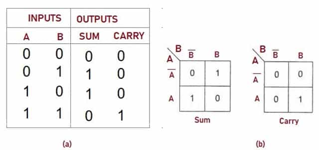
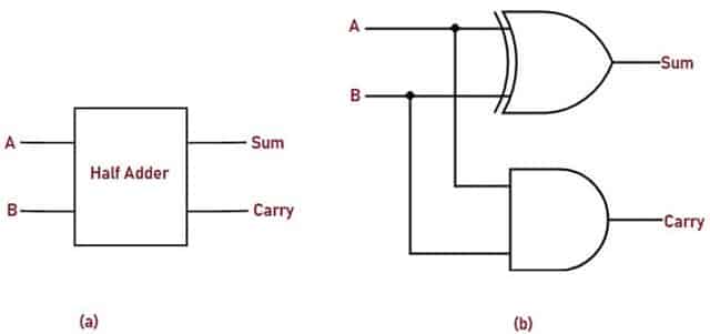
Half Adder is a circuit which adds two binary digits and produces two outputs i.e. Sum and Carry. Fig. 2 shows block diagram and circuit diagram of Half Adder circuit where ‘A’ and ‘B’ are input variables called Augend and Addend bits respectively. Sum ‘S’ and Carry ‘C’ are the two outputs.
Let us examine the possible outcomes of modulo addition for the inputs A and B
If A = 0, B = 0 then Sum = 0, Carry = 0
If A = 0, B = 1 then Sum = 1, Carry = 0
If A = 1, B = 0 then Sum = 1, Carry = 0
If A = 1, B = 1 then Sum = 0, Carry = 1
Fig. 2 – (a) Truth-Table of Half Adder Circuit (b) K-Map Simplification of Truth-Table
 The Truth-Table representation for the inputs is as shown in the Fig. 2 – (a). From the Truth Table, it is clear that the Sum is 1 when the inputs are complementary. The Sum value is 0 when both the inputs are similar. This condition resembles the behavior of ‘XOR’ gate. If we analyse the Carry output, we conclude that when both the inputs are 1, Carry is 1. For rest of the conditions, its ‘0’. The condition for ‘Carry’ resembles the function of ‘AND’ gate. So, we can combine Sum and Carry outputs and implement Half Adder circuit using logic gates as shown in the Fig. 3(b).
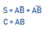
Boolean expression for half Adder’s circuit obtained from K-Map simplification is:
Fig. 3 – (a) Block Diagram (b) Circuit Diagram of Half Adder’s Circuit
Full Adder
When 3 bits need to be added, then Full Adder is implemented. It has three one-bit numbers as inputs, often written as A, B, and Cin where A and B are the operands and Cin is a carry bit from the previous less-significant stage. It adds 3 one bit numbers, out of which two of them are referred to as operands and the third one is referred to as a bit which is carried in. It produces 2 outputs, and they can be referred to as sum and carry output.
A Full Adder’s implementation is a bit difficult when compared to Half Adders. The difference between Half Adders and Full Adders is that the Full Adder’s circuit has three inputs and two outputs, whereas Half Adder’s circuit has only two inputs and two outputs. Here, A and B are the first two inputs and the third input is Carry-In (Cin). Once a Full Adder’s logic is designed, we can string eight of them together to create a byte-wide adder and cascade the carry bit from one Adder to the next.
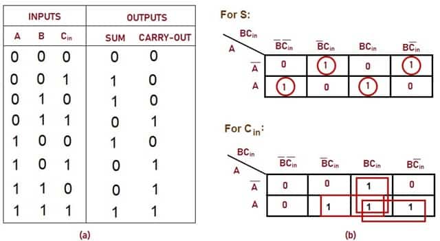
Let us examine the possible outcomes of modulo addition for the inputs A, B, Cin
If A = 0, B = 0, Cin = 0 then Sum = 0, Carry-Out = 0
If A = 0, B = 0, Cin = 1 then Sum = 1, Carry-Out = 0
If A = 0, B =1, Cin = 0 then Sum = 1, Carry-Out = 0
If A = 0, B = 1, Cin = 1 then Sum = 0, Carry-Out = 1
If A = 1, B = 0, Cin = 0 then Sum = 1, Carry-Out = 0
If A = 1, B = 0, Cin = 1 then Sum = 0, Carry-Out = 1
If A = 1, B = 1, Cin = 0 then Sum = 0, Carry-Out = 1
If A = 1, B = 1, Cin = 1 then Sum = 1, Carry-Out = 1
From the Truth-Table, it is clear that the output Sum ‘S’ is XOR operation between the input A and the Half Adder’s Sum output with B and Cin inputs. The overall Carry-Out (Cout) will only be ‘True’ if any of the two inputs out of the three are HIGH.
Fig. 4 – (a) Truth Table of Full Adder’s Circuit (b) K-Map Simplification of Truth Table
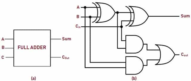
The Full Adder’s circuit can be implemented using the Truth Table and K-Map simplification. This circuit can be constructed by combining two Half Adders. Initially, first Half Adder’s circuit will be used to add inputs A and B to produce a partial sum. The second Half Adder’s circuit can be used to add input carry Cin to the sum produced by the first Half Adder, in order to get the final output ‘S’. If any one of the Half Adder’s logic produces a Carry, then there will be an output carry. So, Cout will be an OR function of both Half Adder’s Carry outputs. The larger logic diagrams can be implemented practically with the above mentioned Full-Adder logic circuit.
Fig. 5 shows Block Diagram and Circuit Diagram of Full Adder’s Circuit. With this type of construction, we can add two bits together, taking a carry from the next lower order of magnitude, and sending a carry to the next higher order of magnitude. In a computer, where multi-bit operation is involved, each bit must be represented by a Full Adder and must be added simultaneously. Thus, to add two 8-bit numbers, we will need 8 Full Adders which can be formed by cascading two of the 4-bit blocks.
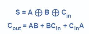
Boolean expression for Full Adder’s Circuit obtained from K-Map Simplification is:
Fig. 5 – (a) Block Diagram (b) Circuit Diagram of Full Adder’s Circuit
How does Adder’s Circuit Work
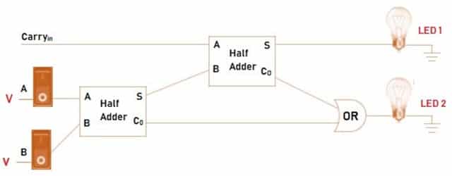
To understand the working principle of an Adder circuit, Let us consider a Full Adder’s circuit implemented using 2 Half-Adders as shown in the Fig. 6. To verify the circuit, power connections are connected through ‘Switches’ to the inputs A and B. The output for each logic gate is displayed using LED.
Logic High = +5 V or Switch is “ON”
Logic Low = 0 V or Switch is “OFF”
The Truth-Table for Full Adders as shown in the Fig. 4 is verified experimentally.
Example:
If A = 00 = Switch is ‘OFF’
B = 0 = Switch is ‘OFF’
Cin = 1= Switch is ‘ON’
  then Sum = 1 = LED 1 turns ‘ON’, Carry-Out = 0 = LED 2 turns ‘OFF’
Fig. 6 – Working Principle of Full Adder’s Circuit using Two Half Adders
Applications of Adder
The applications of Adders are:
- A Full Adder’s circuit can be used as a part of many other larger circuits like Ripple Carry Adder, which adds n-bits simultaneously.
- The dedicated multiplication circuit uses Full Adder’s circuit to perform Carryout Multiplication.
- Full Adders are used in ALU- Arithmetic Logic Unit.
- In order to generate memory addresses inside a computer and to make the Program Counter point to next instruction, the ALU makes use of Full Adders.
- Full-Adders are a part of Graphics Processing Unit for graphics related applications.
Advantages of Adders
The advantages include:
- Half Adder’s design is very simple. It is the basic building block for single bit addition.
- Just with an inverter gate, Half-Adders can be converted to Half Subtractors.
- Full swing output can be obtained with Full-Adders.
- Power consumption is low.
- Speed is high.
- Robustness to supply voltage scaling.
Disadvantages of Adders
The disadvantages are:
- It does not incorporate (or take care of) previous carry for addition.
- Hence it is not suitable for cascading for Multi-bit addition.
- To get rid of this problem, Full Adders are required which add three 1 bit.
- When Full Adders are used in a chain structure such as a Ripple Adder, the output drive capability is reduced.
Also Read:
Logic Gates – Types, Working Principle, Application, Advantage
Transistor – Classification, Configuration, Applications, Advantages
PNP Transistor – Working Principle, Characteristics & Applications
T FLIP FLOP - Construction/ Design, Working Principle and Applications


