PNP Transistor is a sub-type of Bipolar Junction Transistors (BJT’s). It is a basic transistor and often used in various electronic circuits. It is used for functions such as amplification of signal, switches and oscillators. This post provides a detailed information about PNP Transistor, how PNP transistor works, its characteristics, applications, advantages and disadvantages.
What is PNP Transistor
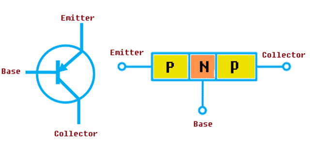
A PNP Transistor is a type of Bipolar Junction Transistor which is composed of three layers where ‘N’ doped layer is sandwiched between two ‘P’ doped layers. In PNP Transistors the electrons are minority charge carriers and holes are majority charge carriers. The current flow is due to the movement of holes. It has two PN junctions:
- Emitter-Base Junction
- Collector-Base Junction

Fig. 1 – Introduction to PNP Transistors
The small Base current has the ability to control large Emitter current, as it is current controlled device. The structure is opposite to NPN transistor but similar in operation.
The PNP Transistor symbol shows an arrow pointing inwards from Emitter to the Base which indicates the direction of the conventional current flow. A PNP Transistor is considered ‘ON’ when the Source Voltage connected to the Base is low and turned ‘OFF’ when it is high.
Fig. 2 – PNP Transistor Symbol
How PNP Transistor Works
To understand the working of a Transistor, it is necessary to know the characteristics of semiconductors.
The fourth column of the periodic table contains certain elements which behave like both conductors and insulators under controlled conditions. These elements are called semi-conductors. Electrons travel slowly in a semiconductor and holes move more slowly than electrons. Only a few donor or acceptor atoms are required to produce changes in the resistivity of a semiconductor.
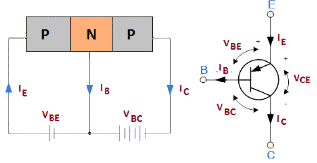
PNP Transistor works when Base Emitter junction is forward biased and the Base Collector junction is reverse biased. A junction is said to be forward biased when a P-type semiconductor is connected with the positive terminal and N-type semiconductor is connected to the negative terminal. In reverse biasing, the P-type semiconductor is connected with the negative terminal and N-type semiconductor is connected to the positive terminal.
Fig. 3 – Construction and Circuit Symbol of PNP Transistor
The Base Collector region is reverse biased which uses external voltage source. This means that the Base is at higher potential than the Collector. Reverse biasing creates no diffusion and hence no current flows between the terminals.
The Base Emitter region is forward biased so that the voltage at the Emitter is at higher potential than at the Base (VBE). Holes are pushed in the Emitter (P-region) crossing the depletion region into the base from positive terminal of the voltage source (VBE). As the Emitter is highly doped, it attracts lot of electrons that diffuse into the Base region.
At the same time, electrons flow from negative terminal pushing the electrons near the Emitter-Base junction into the Emitter. This causes the current (IE) to flow from Emitter to Collector.
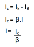
The Collector Current or the Base Current can be calculated using the formula,
The Base is more negative than the Emitter by approximately 0.7 volts for Silicon semiconductor and 0.3 volts for Germanium semiconductor.
To summarize, increasing the forward bias voltage, the Emitter-Base junction barrier is reduced. This allows more carriers to reach the Collector which in turn increases the current flow from Emitter to Collector. It also implies that reducing forward bias voltage decreases the current flow.
Read about PN Junction, Forward Biasing, Reverse Biasing and Depletion Layer
PNP Transistor Characteristics
The relationship between DC currents and voltages are represented graphically, which are known as characteristics. The two important characteristics of a PNP Transistor are:
- Input Characteristics
- Output Characteristics
Input Characteristics for Common-Base Configuration
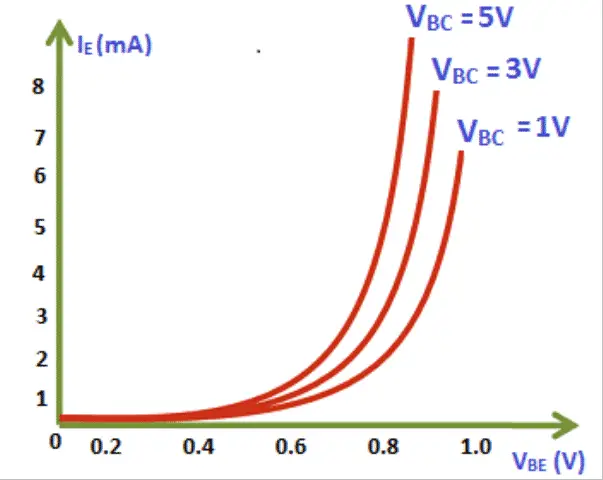
In Common-Base Configuration, for various constant values of Output Voltage (VBC), the curve is plotted between Input Current (IE) versus Input Voltage (VBE).
The figure below shows approximated plot for Input Characteristics. From this characteristic curve we can infer that for fixed value of Output Voltage (VBC), the Emitter Voltage is directly proportional to the Emitter Current (IE).
Fig. 4 – Input Characteristics for Common Base Configuration
Output Characteristics for Common-Base Configuration
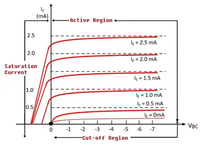
For various constant values of Input Current (IE), the curve is plotted between the Output current (IC) and Output Voltage (VBC). The figure below shows the output characteristics with three regions of interest stated as Active region, Cut-off region and Saturation region. The transistor acts as an ‘OFF’ switch in cut-off region and ‘ON’ switch in saturation region.
Fig. 5 – Output Characteristics for Common Base Configuration
- In Active region, the Base Emitter junction is forward biased and Collector Base junction is reverse biased.
- In Cut-off region, both the Base Emitter junction and Collector Base junction are reverse biased.
- In Saturation region, both the Base Emitter junction and Collector Base junction are forward biased.
Applications of PNP Transistor
The applications of PNP Transistors include:
- They are used in designing amplifier circuits such as Class-B amplifiers.
- They are used in general motor control.
- PNP Transistors are widely used in Darlington pair circuits.
- They are used as switches.
- They are used as oscillators.
Advantages of PNP Transistor
The advantages of PNP Transistors are:
- PNP Transistors are used to source current.
- Makes the circuit design simpler as it generates signal referenced to negative power supply rail.
- Like other transistors, it’s smaller in size and can be a part of Integrated Circuits.
- They generate less noise than NPN Transistors.
Disadvantages of PNP Transistor
The disadvantages of PNP Transistors are:
- PNP Transistor is comparatively slower than NPN Transistor.
- They cannot operate on higher frequencies.
- Performance levels are lower compared to NPN Transistors.
Also Read:
Unijunction Transistor (UJT) - Construction, Working, Characteristics Curve & Applications
Solid State Drive (SSD) – How it Works, Types, Application, SSD Vs HDD
Multiplexer (Mux) – Types, Cascading, Multiplexing Techniques, Application

