Parallel Adder is a digital circuit that efficiently adds more than 1 bit binary numbers. Parallel Adders are implemented using Full Adders. This post will discuss about what is Parallel Adder, how it works, its various types with working principle, applications, advantages and disadvantages.
What is Parallel Adder
In modern Integrated Circuits, the most basic and widely used component are Binary Adders. Adder circuit is classified as Half Adder and Full Adder. The Adder circuit is expected to compute fast, occupy less space and minimize delay. Hence Parallel Adders were implemented with the help of Full Adder circuits.
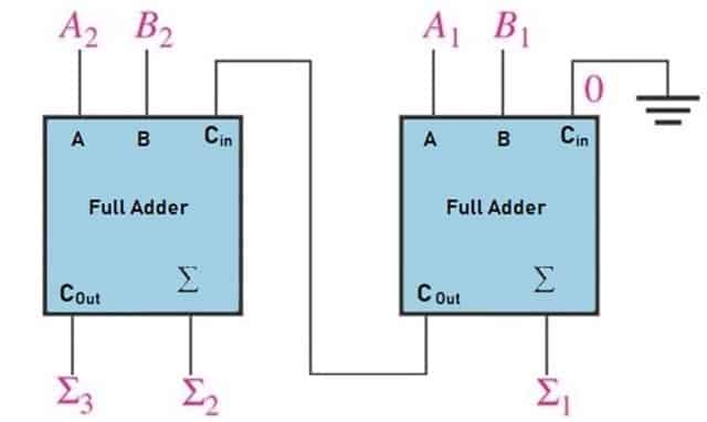
Fig. 1 – Introduction to Parallel Adder
Parallel Adder consists of Full Adders connected consecutively. The input of the Full Adder is the carry bit from the previous Full Adder. ‘n’ Full Adders are required to perform Addition operation. Example: For 4-bit number, 4 Adders are required. Fig. 2, shows schematic diagram of Parallel Adder.
Fig. 2 – Schematic Diagram of Parallel Adder
How does Parallel Adder Work
To understand the working principle of Parallel Adder, Let us understand the construction of Parallel Adder as shown in the Fig. 3. 4- bit Parallel Adder is designed using 4 Full Adders FA0, FA1, FA2, FA3 . Full Adder FA0 adds A0, B0 along with carry Cin to generate Sum S0 and Carry bit C1 and this Carry bit is connected to FA1.
FA1 accepts this Carry C1 and adds with its inputs A1 and B1 to generate Sum S1 and Carry C2. This bit C2 is connected to FA2. This process continues till last Full Adder. FA ‘n’ accepts the carry bit Cn and adds with its input An and Bn to generate the final output along with the last carry bit Cout.
Fig. 3 – Construction of Parallel Adder using Full Adders
Types of Parallel Adder
There are different types of Parallel Adders as listed below:
- Ripple Carry Adder or Carry Propagate Adder
- Carry Skip Adder
- Carry Look Ahead Adder
- Carry Save Adder
- Carry Increment Adder
- Carry Select Adder
Ripple Carry Adder or Carry Propagate Adder
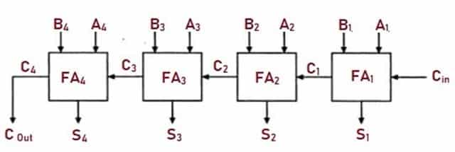
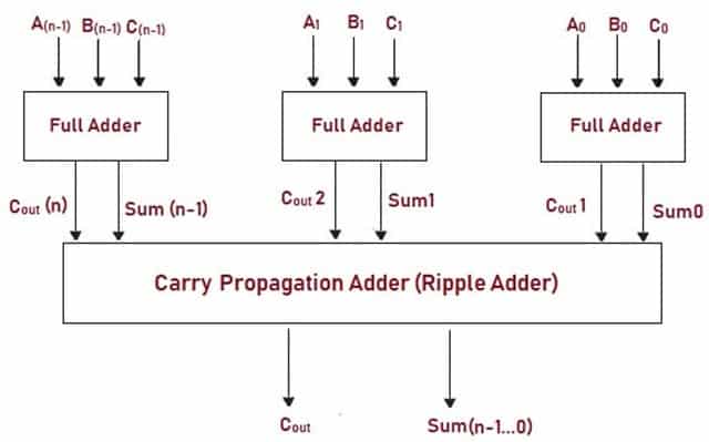
The Ripple Carry Adder is constructed by connecting Full Adders in series. The Carry-Out bit of one stage acts as input to the Carry-In of the next stage. It is also called as Carry Propagate Adder as the Carry bit is propagated. Figure 4 shows the schematic diagram of 4-bit Ripple-Carry Adder. The Augend bits of A are added to the Addend bits of B and generates a sum and carry out. The Carry Out is propagated to the Carry in of the next higher-order bit. The final output generated is a sum of four bits and a carry out (C4).
Fig. 4 – Ripple Carry Adder
Carry-Skip Adder
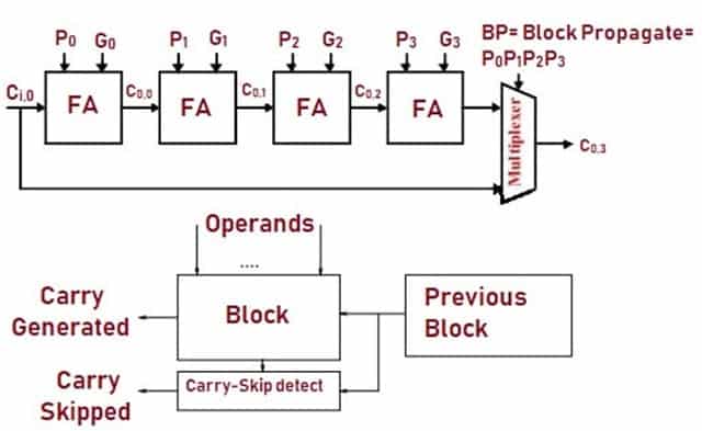
A Carry-Skip adder is also known as a Carry-Bypass Adder. This type of Parallel Adder is designed to improve the delay of Ripple Carry Adder. Carry-Skip Adder is implemented by dividing the stages into blocks and Carry-Skip logic is added to each block. Propagation is skipped without waiting for Rippling. The Carry-Skip logic circuit is faster compared to other circuits.
Fig. 5 – Carry-Skip Adder
Carry Look Ahead Adder
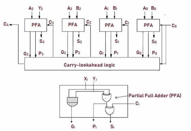
For the given set of inputs (A and B), output signals (P and G) are generated from each cell. Each Cell can be called as Partial Full Adder which consists of X-OR and AND gate.
The Carry Look Ahead (CLA) logic circuit block consists of four 2-level implementation logic circuits which generate carry signals (C1, C2, C3, and C4). Output Sum signal (Si) is generated by using the expression (Si = Pi ⊕ Ci) after a delay.
Fig. 6 – Carry Look Ahead Adder
Carry Save Adder
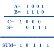
As the name suggests, In Carry Save Adder circuit, carry bits are saved at each stage and hence delay is constant. The carry bit is not propagated but saved at each stage of Adder. At the final stage all the carry bits should be added to obtain output (N-bit Sum). Let us consider an example of 4bit Carry Save Parallel Adder having inputs: A=1 0 0 1 and B=1 1 1 0.
In this type of parallel addition, Sum and Carry are calculated separately unlike conventional addition system. Hence there is no Carry propagation.
Fig. 7 – Carry Save Adder
Carry Increment Adder
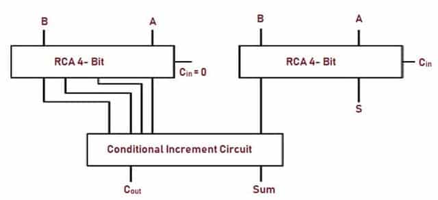
The Carry Increment Adder circuit consists of Ripple Carry Adders and incremental circuitry. Fig 7 shows block diagram of Carry Increment Adder where the inputs A and B of 8 bits are added using 4-bit Ripple Carry Adders. The bits are added in parallel assuming carry input to be 0. After adding higher 4 bits and lower 4 bits of A and B respectively, the conditional increment increases the value of higher 4-bit numbers by 1 and the carry occurs in lower bits. When no carry occurs, higher 4 bit numbers are summed as output.
Fig. 8 – Carry Increment Adder
Carry Select Adder
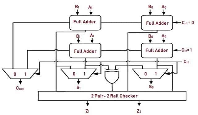
The design of Carry Select Adder consists of multiple pairs of Ripple Carry Adders (RCA) that generates partial sum and carry. Multiplexers (mux) selects the final sum and carry output. This Parallel Adder circuit also reduces propagation delay.
In this type of Adder, the circuit is divided into modules or groups. Each group consists of two Full Adders. One is responsible for evaluating sum and carry for Cin=0 while the other evaluates the sum and carry for Cin=1.The output for Cin=0 and Cin=1 is fed to multiplexer. Sum and Carry is selected based on the carry out of the previous group. 2 Rail 2 Checker circuit helps in detecting any fault in the circuit.
Fig. 9 – Carry Select Adder
Applications of Parallel Adder
The applications of Parallel Adder include:
- BCD to excess- 1 code converter.
- They are used in the analysis of Multiplication Algorithms. Parallel Cellular Automata Machines (CAMs) are incorporated with Parallel Adder Circuits for Parallel Computing.
- They are also used in VLSI implementation for low power applications.
- Parallel Adders are used in ALU for heavy computing environment.
Advantages of Parallel Adder
The advantages of Parallel Adder are:
- Computation is fast.
- Bits are added simultaneously.
- They are economical.
Disadvantages of Parallel Adder
The major drawback of this Adder is the Propagation Delay. The delay is directly proportional to the length of binary numbers that are to be added.
Also Read:
Adder – Classifications, Construction, How it Works and Applications
Logic Gates – Types, Working Principle, Application, Advantage
Demultiplexer (Demux) – Types, Cascading, Applications and Advantages


