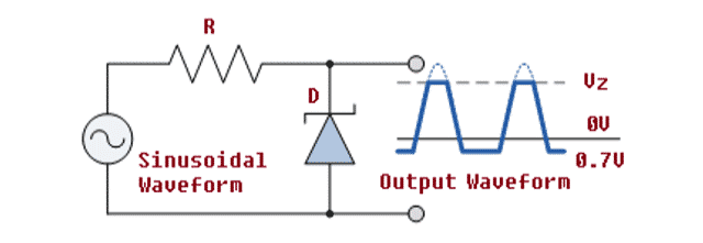
The existence of electronics industry would have been impossible without Diode. It is the simplest semiconductor device which finds its applications all over in the world of electronics. This article will discuss about what is Diode, its brief history, operation modes, VI characteristics, types, applications, advantages and disadvantages.
What is a Diode
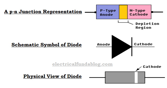
A Diode is a semiconductor device that allows the current flow only in one direction. Diodes are manufactured from a single piece of semiconductor material having two electrodes. A P-type semiconductor is an intrinsic semiconductor doped with a trivalent impurity and N-type semiconductor is doped with pentavalent impurity are fabricated together to form a p-n junction. P-type forms the anode and n-type forms the cathode.
Semiconductors like Silicon (Si), Germanium (Ge) and Gallium Arsenide (Ga As) have electrical properties of both conductors and insulators. Their atoms are closely grouped together in a crystalline pattern called ‘Crystal Lattice’, as they have few free electrons.
Fig. 1 – PN Junction Representation, Schematic Symbol and Physical View of Diode
They can conduct large amount of electricity by adding impurities to this crystalline structure which produces more free electrons than holes and vice versa. These impurities are called Donors or Acceptors. The process of adding impurity atoms to semiconductor atoms is known as Doping.
Silicon is the most commonly used semiconductor.
How a Diode Works
In a p-n junction, the p-region has high concentration of holes and very few electrons. Whereas the n-region has high concentration of electrons and few holes. A process called diffusion takes place wherein the free electrons from n-region diffuse in to the p-region combining with holes leaving positive ions in the n-side.
Few atoms on the p-region converts in to the negative ions. Similarly few atoms on the n region are also converts to positive ions. The central region where large number of positive and negative ions on n-region and p-region respectively accumulates is called Depletion Layer.
The process of diffusion creates a static electric field across the pn junction of the diode called as “Barrier Potentialâ€. The Barrier Potential opposes the flow of positive and negative ions across the junction.
Fig. 2 – Unbiased PN Junction Diode
For the diodes to work, an external DC voltage is applied to assist the flow of charge carriers through the Depletion layer. This method of applying external DC Voltage is called biasing. It is set to be forward biased when the P- side (Anode) is connected to the positive terminal of the supply and n side (cathode) is connected to the negative terminal of the supply. Similarly, if n-side (cathode) is connected to the positive terminal and p-side (anode) is connected to the negative terminal, then it is called reverse bias.
Generally a resistor is connected in series with diodes to limit the current flow.
Operation Modes of a Diode
There are two operation modes of diodes based on the applied voltage. They are:
- Forward bias
- Reverse bias
What Happens When a Diode is Forward Biased
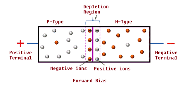
In forward biasing, the negative terminal is connected to n-region which makes the electrons move towards p-region. Similarly, connecting the positive terminal to p-region makes the holes from p-region to move towards n-region.
Due to this movement of electrons and holes, neutral atoms are formed. Reduction in barrier potential reduces the width of the depletion region and with the increase in supply voltage more atoms are converted into neutral atoms and less charged ions are available in the region. The width of the depletion region is further reduced.
Fig. 3 – Diode in Forward Bias
The conversion of atoms to neutral atoms continues till the depletion region collapses and hence large number of electrons and holes crosses the junction and the current flows from anode to cathode. The electrical resistance of a forward biased diode is very small and voltage drop is negligible across it. The forward voltage value for silicon diodes is about 0.7V.
To summarize:
- Electrical resistance is low
- Current flows only in forward bias condition.
- The diode acts like a short circuit.
What Happens When a Diode is Reverse Biased
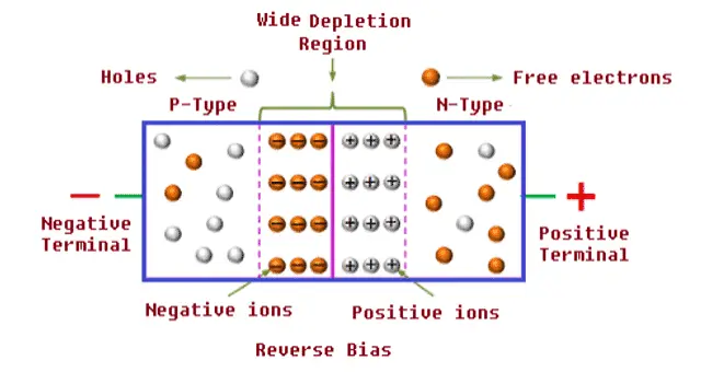
When the diode is reverse biased i.e. when the n-region (cathode) is connected to positive terminal and p-region (anode) is connected to negative terminal, the negative terminal attracts the holes from the p-region and positive terminal attracts the electrons from the n-region.
The depletion region widens which opposes the current flow. The resistance of the diode is infinite and no current flows when it is reverse biased and small leakage current flows through the junction.
Fig. 4 – Diode in Reverse Bias
To summarize:
- Electrical resistance is high compared to forward bias.
- No current flows in reverse bias condition.
- The diode acts like an open circuit.
VI Characteristics of PN Junction Diode
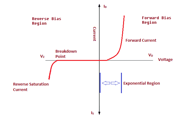
The VI characteristics of a PN Junction Diodes can be categorized into two parts i.e. VI characteristics during Forward Bias and Reverse Bias. The figure below shows the Voltage-Current characteristics in diodes.
Fig. 5 – VI Characteristics of PN Junction Diode
VI Characteristics of Diode in Forward Bias
The non –linear curve indicates that when the p-n junction is forward biased, the electrical resistance, impedance is low and conducts a large amount of current known as infinite current.
In forward bias region, the VI characteristics is explained with the equation:
Here, VT = KT/q
Where,
- ID = Forward current
- Is = Saturation current
- VT = Forward voltage
- K = 1.38×10⁻²³(Boltzmann’s constant)
- T = Absolute Temperature
- q = 1.6×10 -19 (electronic charge)
- n = a constant and has a value of 1 or 2 which depends on the material and physical structure of the diodes.
- n=1 for Silicon and Germanium
- n=2 for Gallium Arsenide.
VI Characteristics of Diode in Reverse Bias
The current in reverse bias is low till breakdown is reached and hence diode looks like an open circuit. When the input voltage reaches breakdown voltage, reverse current increases enormously.
The current value (ID= – IS) is so small that we can approximate it to zero.
Hence We can Say that:
- ID ≈ 0 if –VZK < VD << -n VT
- ∴ VD ≈ 0.7 if ID >0 ( Forward bias)
- ID ≈ 0 if – VZK < VD < 0 (Reverse bias)
Types of Diodes
There are numerous types of diodes that are specifically designed or modified for specific applications. Below is a list of some popular diodes.
- Zener Diodes
- Photo Diodes
- Light emitting Diodes
- Schottky-Barrier Diodes
- PIN Diodes
- Backward diodes
- Baritt Diodes
- Gunn Diodes
- Step recovery Diodes
- Tunnel Diodes etc.
Fig. 6 – Types of Diodes
Applications of Diode
Diodes are mainly used in rectifiers, clippers, clampers, snubber circuits and voltage regulators. Its few applications along with Circuit diagram is explained below.
Use of Diode as Rectifier
Conversion of AC input voltage to the DC output voltage when AC voltage is applied to a diode is called as rectification. Diodes are used individually or connected together to produce various rectifier circuits such as half-wave and full-wave rectifiers for power and signal rectification.
Fig. 7 – Diode Rectifier Circuit
Use of Diode as Clipper
Clipping is a waveform shaping where the input signal is clipped or cut to produce an output which is a flattened version of the input signal. Diode-clipping circuits are used in voltage limiting applications as this circuit eliminates voltages below zero.
Fig. 8 – Diode Clipper Circuit
Use of Diode for Clamping
An electronic circuit that prevents the signal from exceeding a certain defined value is known as a clamping circuit. Diode’s clamping circuits are used as voltage multipliers and to remove distortions in the signal.
Fig. 9 – Diode Clamping Circuit
Advantages of Diode
The advantages of Diodes include:
- Diodes are compact in size and compatible.
- Designing electronic circuit is simple with certain diodes like Zener diodes.
- Diodes help in controlling the current flow.
- These diodes produce less unwanted noise.
- Certain diodes like Schottky diodes can operate at high frequencies.
- Light emitting diodes are highly efficient compared to other diodes and they can emit light of the expected colors.
- Operates at high switching speed.
Disadvantages of Diodes
The disadvantages of Diodes include:
- Power dissipation is more for Zener diodes and hence it is less efficient for heavy loads.
- Diodes are highly sensitive to temperature.
- Amplification is necessary in photodiode based circuits.
- Light emitting diodes are expensive compared to other diodes.
- Certain diodes like Schottky diodes have low maximum reverse voltage
- They have high reverse current and impedance.
Also Read:
What is CAPTCHA Code – How it works, Design, Types, Applications
What is Smart card – How it Works, Specifications, Types and Applications
OSI Model – Characteristics of Seven Layers, Why to Use & Limitations

