Shift Registers which are designed using Flip-Flops are the devices that stores and transfers the data bits. This post provides a detailed explanation about Shift Registers, its modes of operation, types, working principle, applications, advantages and disadvantages.
What are Shift Registers
Shift Registers are basically a type of sequential logic circuit used to “store” and “shift”/ “transfer” data bits either in serial or parallel or a combination of both serial and parallel. They are basically configured using Flip-Flops in sequence where the output of one Flip-Flop becomes input to the other.
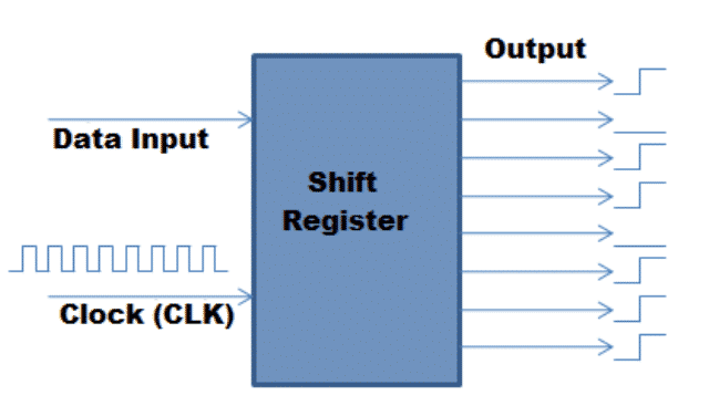
Flip-Flops make an ideal choice in designing them as they are edge- triggered devices and can retain output state. Fig. 1 below shows the schematic diagram of Shift Register.
Fig. 1 – Schematic Diagram of Shift Register
Modes of Operation of Shift Registers
There are four basic modes of operation based on the movement of data in the Registers and they are:
- Serial In – Serial Out (SISO) Mode
- Serial In – Parallel Out (SIPO) Mode
- Parallel In – Serial Out (PISO) Mode
- Parallel In – Parallel Out (PIPO) Mode
Serial in – Serial Out (SISO) Mode
SISO mode accepts data serially under clock control i.e. the data transmitted is one bit at a time in either left or right direction. The stored information is produced as its output. Fig. 2 below shows a SISO mode of Shift Register consisting of 4 D-Type Flip-Flops (FF0, FF1, FF2 and FF3). They are connected serially with the same clock (CLK) signal applied to each Flip-Flop.
Fig. 2 – Schematic of Serial In – Serial Out (SISO) Mode
Serial In – Parallel Out (SIPO) Mode
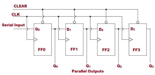
The SIPO mode of Shift Registers accepts data serially i.e. one bit at a time through a single data line and produces a parallel output. Fig.3 shows a SIPO mode consisting of 4 D-Type Flip-Flop’s (FF0, FF1, FF2 and FF3). In addition to the CLK Signal, Clear (CLR) signal is also connected to all the Flip-Flops to ‘RESET’ them.
Fig. 3 – Schematic of Serial In – Parallel Out (SIPO) Mode
Parallel In – Serial Out (PISO) Mode
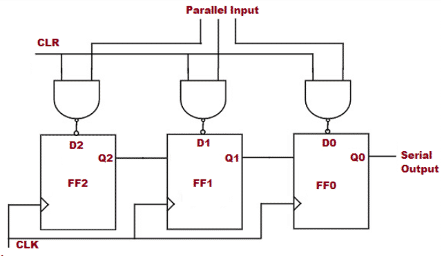
PISO mode of Shift Registers allows parallel data input i.e. data is fed separately to each input of Flip Flop and produces a required serial output. A Multiplexer is connected at the input of each Flip-Flop. The previous output and the parallel data input are connected to the input of the Multiplexer and output of the Mux is connected to the next Flip-Flop. Since the same CLK signal is applied, all the Flip-Flops are synchronous with each other.
Fig. 4 – Schematic of Parallel In – Serial Out (PISO) Mode
Parallel In – Parallel Out (PIPO) Mode
In PIPO mode of Shift Registers, there is no serial shifting of the data and hence the Flip-Flops are not interconnected. The input and output to each Flip-Flop is separate. All the 4 Flip-Flops are connected to the same Clock (CLK) and Clear (CLR) signal.
Fig. 5 – Schematic of Parallel In – Parallel Out (PIPO) Mode
Types of Shift Registers
Shift Registers are classified into five types which are listed below:
- Shift Right Register
- Shift Left Register
- Bidirectional Shift Register
- Circular Shift Register
- Linear Feedback Shift Register
Shift Right Registers
These Registers shifts the data in the right direction.
Shift Left Registers
These Registers shifts the data in the left direction.
Bidirectional Shift Registers
The data movement in this type of Registers is in both the directions i.e. from Left to Right and Right to Left.
Circular Shift Registers
These type of Registers can be created by connecting the serial input and the last output of a Shift Register.
Linear Feedback Shift Registers
The input bit to this type of Register is a linear function of its previous stage i.e. output of the previous Flip-Flop.
How Does Shift Registers Work
To understand the operation or the working principle, Let us consider a four-bit Shift Register in which data movement is from left to right. It is basically designed using D Flip-Flops and they are connected in such a way that the output of one stage becomes input to the next stage.
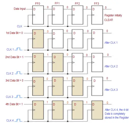
Fig.6 shows illustration of four bits of data entered serially at the input of D Flip-Flop. Let us assume data to be ‘1010’. The Register is initially cleared, forcing all four outputs to zero and then the input is applied sequentially to first Flip-Flop on the left (FF0). One bit is transmitted from left to right for every clock pulse which acts as a common input to all the Flip-Flops.
Each Flip-Flop can store one bit (either ‘0’ or ‘1’) and least significant bit of the data is shifted through the registers i.e. from FF0 to FF3. To obtain the data out of the register, they must be shifted out serially. This can be done by ” Destructive Readout” i.e the original data is lost and all the Flip-Flops are Reset to zero. After 4th CLK signal, Data is completely stored in the Register.
Fig. 6 – Illustration of Shifting of Data Serially
Applications of Shift Registers
The applications include:
-
They are basically used for data transfer and temporary data storage.
-
They are implemented in devices like computers and calculators as they serve as temporary data storage spaces.
-
They were used to handle data processing in the former years of Computer Technology. Example: Shift Right and Left, Arithmetic Shift Right and Left, Rotate Right and Left were supported by the processor.
-
They are used to add more binary inputs to a Microprocessor as it has fixed number of I/O pins.
-
They are also used as Delay Circuits.
-
They are used as Sequence Generator and Counters.
-
In Digital transmission, they act as Parallel to Serial Converter at the transmitter end (Multiplexing) and Serial to Parallel Converter at the receiver end (Demultiplexing).
Advantages of Shift Registers
The advantages include:
- They operate faster than the logic circuits in converting Serial to Parallel and Parallel to Serial interfaces.
- PN (Pseudo Noise) Sequence number in CDMA (Code Division Multiple Access) is generated using them.
- They are easy to design as it reduces the amount of wiring and occupy less space.
- They are helpful in tracking the information (data).
- Delaying a signal is easy.
- Data Encryption and Decryption can be achieved using linear Feedback Shift Registers.
Disadvantages of Shift Registers
The major drawback is that the output current of Register is limited.
Also Read:
OSI Model - Characteristics of Seven Layers, Why to Use & Limitations
Hamming Codes - How it Works, Application, Advantages & Disadvantages
Barcode Number System - Types, Structure, How it works, Application, Advantage & Disadvantage


