Printed Circuit Design (PCB design) refers to the process of designing the layout and configuration of printed circuit boards (PCBs). Additionally, modern electronics are built on Printed Circuit Boards (PCBs), which act as a foundation for connecting various electrical components. We’ll get into the basics of PCBs, examine important terminologies, understand various classifications, and explore their uses and advantages in this article.
What is PCB (Printed Circuit Board)?
A PCB is a fundamental component in electronic devices, providing a platform for connecting electronic components using conductive pathways, tracks, and pads etched or printed onto a non-conductive substrate.
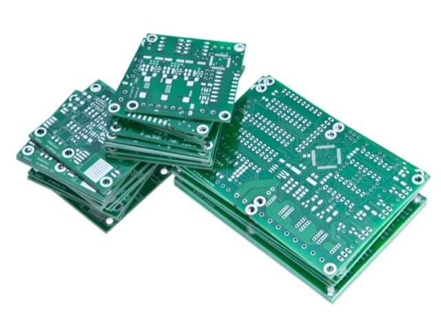
Basically, Printed Circuit Board is a non-conductive, copper-laminated board on which all electronic and electrical components are linked together into a single, physical board that supports each component from the base up. All components are connected by wire when a PCB is not constructed, which adds complexity and reduces circuit reliability.
In this approach, we are unable to create a very big circuit, such as a motherboard. Because every component on a PCB is internally connected and wire-free, the overall complexity of the circuit design is reduced.
Generally, electricity and connectivity between the components are provided by the PCB, which allows the device to operate as intended. PCBs can be tailored to a user’s demands in any way.
Basic Terminologies used in PCB
-
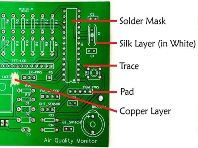
Pad:
To connect components to the printed circuit board (PCB), exposed metal is present in places called pads. Although there are various options for pad design and connection methods, solder is typically used to attach things to the pad’s surface.
-
Trace:
Components on a printed circuit board (PCB) are not connected by wires. Every component is connected using a conducting substance, such as copper. The term “trace” refers to the copper portion of the PCB that connects every component.
-
Silk layer:
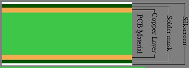
Basically, this layer is used to print lines, letters, or other artwork onto PCB surfaces. The most common ink used for screen printing is epoxy. According to user demand, a silk layer, often referred to as a silk screen top or silk screen bottom, can be utilized in the top or bottom layer of a printed circuit board.
-
Layers:
The user can select the PCB layer based on the application, cost, and available circuit space. Single-layer PCBs are the easiest to design, produce, and utilize in daily life. However, compared to single-layer PCBs, double-layer or multi-layer PCBs are most suited for extremely big and complex circuits. These days, 10–12 layers can be joined in a multi-layer printed circuit board (PCB), with communication between components at separate levels being of utmost importance.
-
Solder Mask:
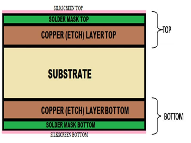
The copper layer has an extra layer on top known as the Solder Mask. Although it can be any color, this layer is often green in color. The purpose of this insulating layer is to keep the pads on the PCB from unintentionally coming into contact with other conducting materials.
-
Top and bottom layers:
Every component is put in the top layer of the PCB. This stratum is often green in color. All of the components are soldered through the hole in the bottom layer of the PCB, which is also referred to as the component lead. Sometimes a solder mask, or green color layer, is applied to the top and/or bottom layers of the printed circuit board.
-
Footprint:
An assembled circuit board’s footprint is a schematic that shows the locations of all the pads and through-holes as well as how the components are supposed to be mounted to the board.
-
Substrate:
The actual substance that contains the components and traces on a PCB is called the substrate. Accordingly, selecting an appropriate substrate is the first step in creating a PCB of high quality. The substrate is typically composed of composite material, epoxy resin, or fiberglass, which act as insulators.
Its characteristics can impact the final product’s performance and dependability, and it forms the basis of the entire printed circuit board. Throughout the PCBs lifetime, the substrate must be able to endure changes in temperature, pressure, and environmental factors. Additionally, it prevents nearby copper layers from shorting together by keeping them insulated.
-
Jumpers:
Jumpers are insulated or non-insulated pins that are utilized as conductors. They can be used in a PCB design to reduce the amount of traces and/or layers in a board design, which lowers PCB costs, or they can be used to create a PCB that can be configured in different ways by removing specific jumpers. Modern PCBs are less likely to contain jumpers than they were in the past while designing PCBs.
Printed Circuit Boards (PCBs) Classifications
PCB can be categorized in many ways based on their design, use, and other characteristics. Selecting the right PCB type for our purpose is necessary, as there are various varieties available. The classifications for printed circuit boards (PCBs) are as follows:
- Classification based on the mounting technology
- Classification based on the number of layers
- Classification based on the type of PCB based on their flexibility
-
a) Classification Based on the Mounting Technology:
Based on mounting technology, there are two kinds, which are as follows:
-
Through-hole PCB:
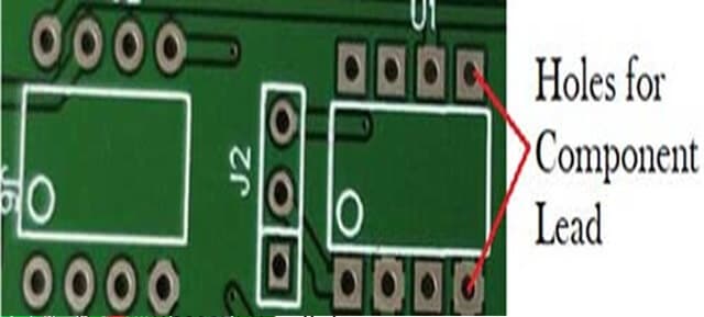
For this kind of PCB, a drill bit must be used to create a hole in the board. Component leads are inserted into these holes and soldered to pads on the PCBs other side. Although drilling through a PCB increases cost, this approach is very dependable for component mounting and provides greater mechanical support for electrical components. PCBs with through holes may tolerate higher levels of strain, vibration, and movement. This mounting approach is simple to use in single-layer PCBs, but it is more challenging to make holes in double- and multi-layer PCBs.
-
Surface-mounted PCB:
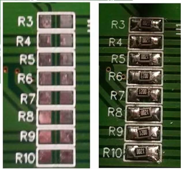
Because these components have very small leads or don’t require any leads at all to be mounted on the board, they are small in size on this kind of PCB. With this technology, there is no need to drill a hole in the board because SMD components are attached directly to its surface.
 b) Classification based on the number of layers:
Based on the number of layers, there are three kinds, which are as follows:
-
Single-Layer PCB:
Another name for a single-layer PCB is a single-sided PCB. Due to their ease of design and production, this kind of PCB is the most popular and basic kind. It has a layer of conducting material on one side. Due to its excellent conducting qualities, copper is often used as the conducting material for printed circuit boards.
The PCB is coated with a solder mask layer to prevent oxidation, and then all of the components are marked out using a silk screen. It connects various electrical and electronic components, such as resistors, capacitors, inductors, etc., on just one side of the board.
  All these components are connected by soldering. These printed circuit boards (PCBs)     are utilized in the mass production of inexpensive devices such as radios, printers, solid-   state drives, and calculators.

-
Double-Layer PCB:
Another name for a double-sided PCB is a double-layer PCB. As the name implies, this kind of PCB has a thin layer of conducting material—such as copper—applied to the board’s top and bottom. Within the PCB, there is a via with two pads positioned in corresponding positions on separate layers of the board. A hole in the board, as seen in the figure, connects these electrically.
This sort of PCB board has several advantages, including greater flexibility, lower cost, and a more compact circuit due to its smaller size. The majority of applications for this sort of PCB include power monitoring systems, industrial controls, converters, UPS systems, HVAC systems, phones, and amplifiers.
-
Multi-Layer PCB:
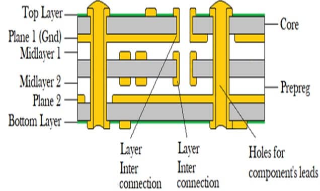
A multilayer printed circuit board comprises more than two layers. This indicates that there are at least three copper-conductive layers on this kind of PCB. In order to ensure that any circuit components are not damaged by excessive heat, glue is positioned between layers of insulation to secure the board.
In extremely small spaces and tiny circuits, this style of PCB design is highly complex and used for huge and difficult electrical tasks. A lot of significant applications, including GPS technology, satellite systems, medical equipment, file servers, and data storage, use this kind of PCB.
  c) Classification based on their flexibility:
Based on flexibility, there are three kinds, which are as follows:
-
Rigid PCB:
These PCBs are designed to prevent twisting and are composed of solid materials. Similar to flex PCBs, rigid PCBs can be single, double, or multi-layered in terms of their layer arrangement. After installation, this PCB’s shape remains unchanged. This PCB is called a rigid PCB because it cannot be bent to fit the curvature of the base.
Since this kind of PCB has a relatively long lifespan, it is used in various computer components, including the CPU, GPU, and RAM. Single-sided rigid PCBs are the most common type of PCB, have a simple design, and are manufactured worldwide. Nine or ten layers can make a multi-layer rigid PCB more compact.
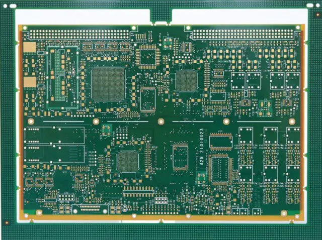
Rigid PCB
-
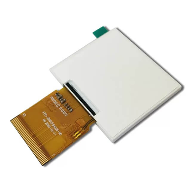
Flexible PCB:
Another name for flexible PCBs is “flex circuit.” Flexible plastic materials such as polyimide, PEEK (polyether ether ketone), or transparent conductive polyester film were utilized to create this sort of PCB. Usually, the circuit board is twisted or folded.
This kind of printed circuit board is extremely complex and has a variety of layers, including single-, double-, and multi-sided flex circuits. Flex circuits are used in the production of organic light-emitting diodes, LCDs, flex solar cells, and complicated electronics like laptops, cell phones, and automobiles.
-
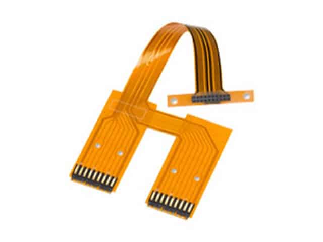
Flexible-rigid Printed Circuit Board:
The most crucial board is the combination of a rigid and flexible circuit. Multiple flexible PCB layers are adhered to several rigid PCB layers to form flex-rigid boards. The figure depicts the flex-rigid board. It is used in many devices, including digital cameras, cell phones, cars, etc.
Benefits of Printed Circuit Boards (PCBs):
The benefits of PCBs are as follows:
 Single-sided PCBs:
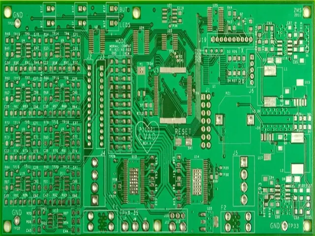
- Due to their less complex designs, single-sided circuit boards can be manufactured at a lower cost because they require fewer resources. This combination makes it possible to produce goods that are both high-quality and reasonably priced quickly and in large quantities.
- Moreover, this makes it easy to construct boards in large quantities, whereas multi-layer boards need more time and labor to produce.
 Double-sided PCBs:
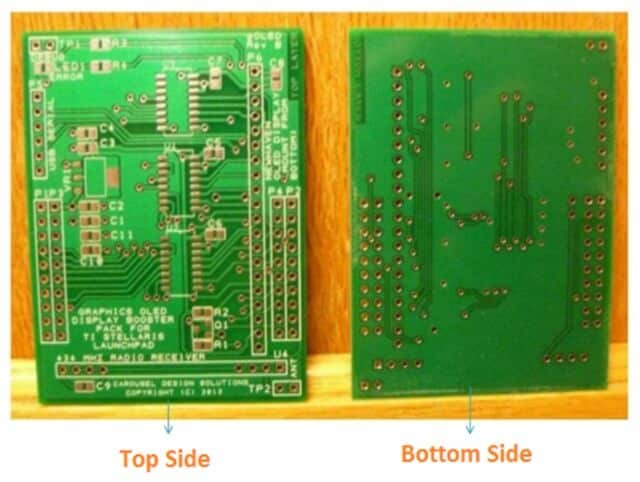
- Due to their high degree of flexibility and simplicity of usage, double-sided PCBs are beneficial. Since components can be positioned on the second layer, they also permit higher circuit densities.
- Double-sided boards produce smaller printed circuit boards (PCBs) that are ideal for lighting or dashboard integration, despite their increased complexity.
- Smaller products can be produced and sold for less money as a result of saving money.
 Multilayer PCBs:
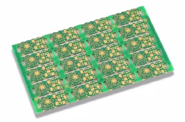
- By shielding delicate components, the multi-layer PCB increases the circuit’s dependability. And in the end, produces a smaller, more compact, and more robust board. By shielding delicate components, the multi-layer PCB increases the circuit’s dependability and, in the end, produces a smaller, more compact, and more robust board.
- Increased durability— layering a design is an excellent approach to adding more security to a strong physical design.
- Overall quality— Although much harder to design and manufacture, this means that the production process is more exacting and requires more attention to detail.
- High-power circuit designs— For complex designs, it may be necessary to design your PCB with numerous layers for certain performance components.
- Space-saving— By stacking conductive layers, a circuit board’s footprint can be lowered, enabling larger circuits to fit on a smaller board.
- Single connection point— A multilayer design has a single input rather than several inputs on separate PCBs.
 Rigid PCBs:
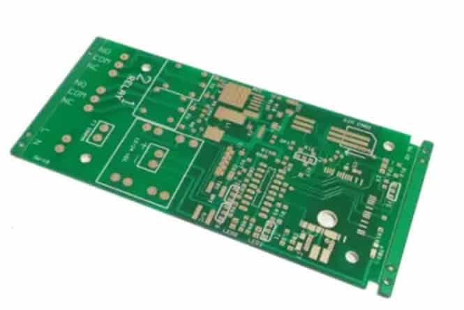
- A rigid PCB is preferable if you want a robust circuit board with more components on it, while flexible PCBs are not as durable as rigid PCBs.
- They can be made in large quantities and at a reasonable cost. More circuit density is also possible with it.
- In products where electronic components must be fixed and able to endure extreme temperatures and stress, rigid PCBs are often used.
 Flexible PCBs:
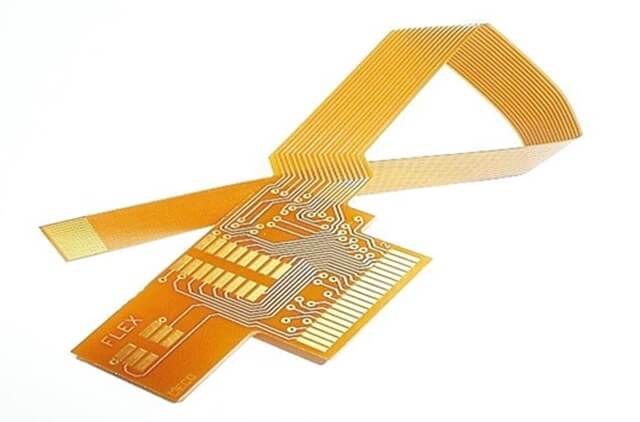
- The use of flexible PCB boards for regular electrical product assembly has a number of advantages, including simplified functions and reduced size. Since flex PCBs are made of a different material than other circuit boards, they require less space and weigh less.
- A product can be made more flexible with the use of flex PCBs, which is advantageous for a range of products. They can tolerate extreme temperatures because their substrates dissipate heat. Because of its architecture, flex PCBs can work with a wide range of components, some of which may be small and inexpensive.
- Additionally, these have connectors that are adaptable to their layout. The best feature is that they may be replaced at a lower cost because they require less packing and material.
 Rigid-Flex PCBs:

- Compact and lightweight, rigid-flex printed circuit boards (PCBs) find extensive use in the aerospace, medical, and consumer electronics industries. Among the advantages are:
- Extreme flexibility
- Reduced space due to 3D.
- Shock resistance
- Increased dependability
- Light weight
- Less solder joints, which improves the reliability of higher connections
- Easy PCB assembly
- These items are suitable for situations where resilience is required, such as in the event of a connector failure, because they can endure high-stress settings.
Applications of Printed Circuit Boards (PCBs)
Some common uses of PCBs are as follows:
-
Communications:
PCBs are the building blocks of many gadgets, including radios, tablets, smart watches, and smartphones.
-
Computers:
Circuit boards are the fundamental component of all computers, smartphones, and navigation devices. In fact, many devices that have screens depend on these small yet crucial elements.
-
Entertainment Systems:
Printed circuit boards are the magic ingredient that makes TVs, stereos, DVD players, and game consoles work.
-
Home Appliances:
PCBs are used in appliances such as coffee makers, refrigerators, microwaves, and alarm clocks.
-
Scanning Equipment:
A solid foundation of circuit boards and copper wires is essential to the operation of all scanning devices, including X-rays, CT scans, and ultrasounds.
-
Monitors:
Circuit boards, batteries, and other electronic components are needed by the devices that measure your blood pressure, heart rate, blood glucose, and other medical equipment.
-
Medical Equipment:
Electronics are frequently used by medical researchers in PCB-containing equipment such as compressors, control systems, microscopes, and other devices.
-
Navigation:
A lot of the gadgets we use today, such navigation systems, are PCB-based. The tiny printed circuit boards needed by the gadgets for operation are included in these systems.
-
Media Devices:
Modern cars come equipped with keyless entry, hands-free phoning, and other features that make driving and using a car safer. All of this is done with electronic components.
-
Control Systems:
Circuit boards are strong instruments for keeping an eye on and controlling various parts of a car. Advanced automotive control systems can be easily created and customized to fit a particular kind of vehicle with the use of circuit boards.
-
Industrial Equipment:
Printed circuit boards are employed in the construction of assembly lines, presses, and ramps in this industry.
-
Power Equipment:
PCB provides everything you need, from industrial applications to home usage power supplies and inverters.
-
Measuring Equipment:
A circuit board is utilized in several machines to regulate temperature, pressure, and other factors related to the production process.
Read Also:
Bridge Rectifier Circuit – Working, Types, Characteristics and Applications
Circuit Breaker – How it Works, Types, Applications and Advantages

qdco7m
Получите бесплатную консультацию юриста на сайте [url=https://pomoshch-yurista11.ru/]юридическая услуги[/url].
Юридические услуги оказывают значительное воздействие на различные сферы жизни. В жизни порой возникают обстоятельства, когда требуется помощь квалифицированного юриста.
Важно знать, что юрист может защитить ваши интересы. В повседневной жизни, например, при составлении contracts, полезно обратиться за консультацией к юристу.
На сайте pomoshch-yurista11.ru вы можете найти услуги опытных юристов. Вы сможете получить помощь по самым разным юридическим вопросам прямо на сайте pomoshch-yurista11.ru.
Профессиональные юридические услуги помогут вам избежать лишних затрат и сэкономить время. Поэтому важно обратиться к специалистам в случае необходимости.
Для получения квалифицированной помощи в вопросах раздела имущества, обратитесь к специалистам на [url=https://razdel-imushchestva33.ru]исковое заявление о разделе имущества после развода[/url].
Опыт юристов позволяет им качественно защищать интересы своих клиентов.
a3tnx2
credit card starting with 5 [url=https://otvetnow.ru]https://otvetnow.ru[/url] homeowners insurance atlanta
Hi there! This is my first visit to your blog! We are a team of volunteers and starting a new project in a community in the same niche. Your blog provided us beneficial information to work on. You have done a wonderful job!
hey there and thank you on your info – I’ve certainly picked up anything new from right here. I did however expertise some technical issues using this web site, as I skilled to reload the site many times previous to I may get it to load correctly. I were puzzling over if your hosting is OK? Now not that I’m complaining, however slow loading instances instances will often have an effect on your placement in google and can injury your high-quality rating if ads and ***********|advertising|advertising|advertising and *********** with Adwords. Anyway I’m adding this RSS to my e-mail and could glance out for much more of your respective exciting content. Make sure you update this once more very soon..
Hi there, just became alert to your blog through Google, and found that it is really informative. I am gonna watch out for brussels. I will appreciate if you continue this in future. Many people will be benefited from your writing. Cheers!